Light source

a technology of light source and phosphorescent light, applied in the field of light source, can solve the problems of high panel fabrication cost and complex panel fabrication process, and achieve the effect of increasing the utilization rate of phosphorescent light emission and high-luminance light emission

Inactive Publication Date: 2006-09-28
NGK INSULATORS LTD
View PDF9 Cites 5 Cited by
  • Summary
  • Abstract
  • Description
  • Claims
  • Application Information

AI Technical Summary

Benefits of technology

[0008] It is an object of the present invention to provide a light source comprising electron emitters for increasing the rate of utili

Problems solved by technology

All of these disclosed electron emitters are disadvantageous in that since no dielectric body is employed in the emitter, a forming process or a micromachining process is re

Method used


Image

  • Light source
  • Light source
  • Light source

Examples


first embodiment

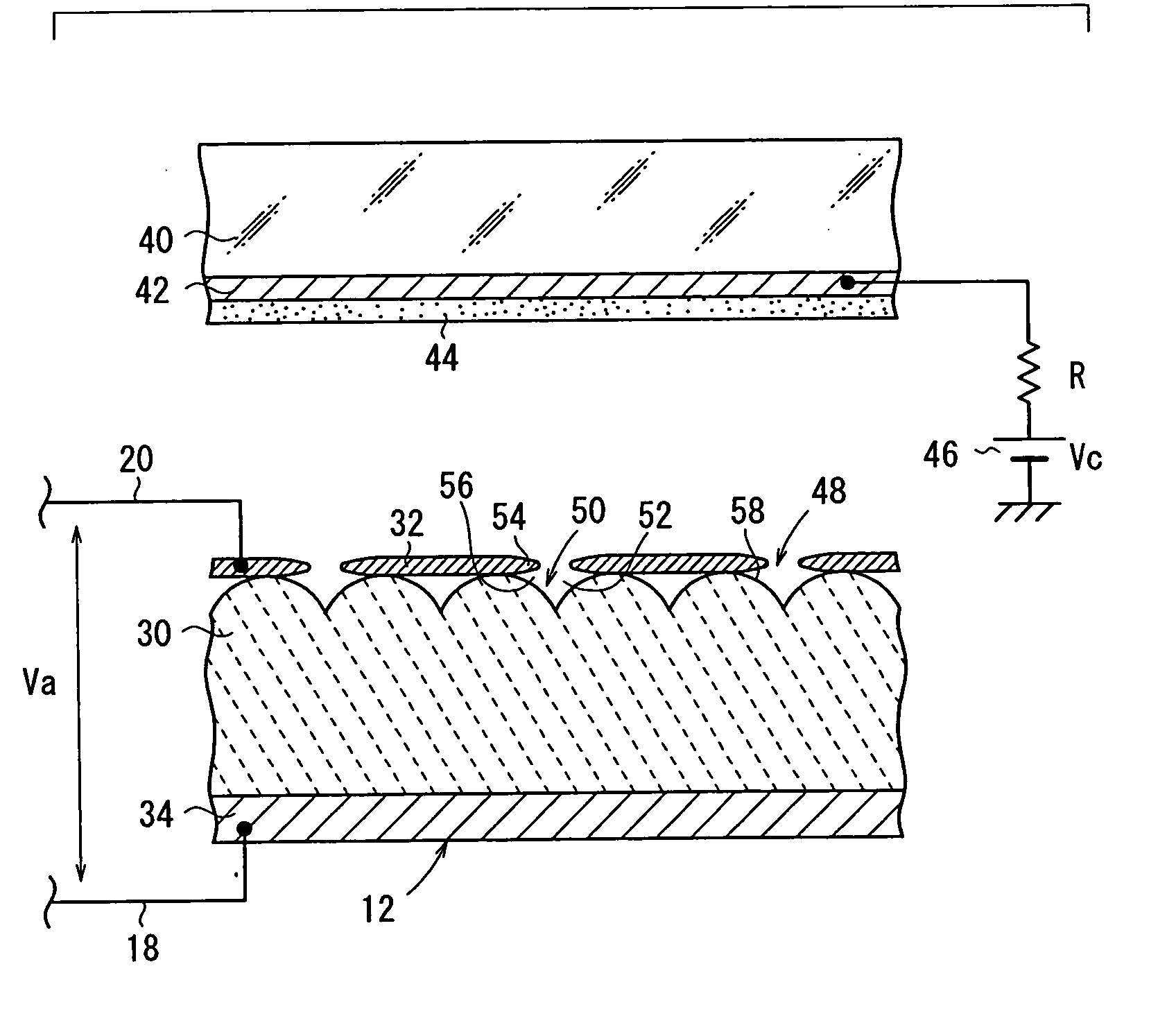
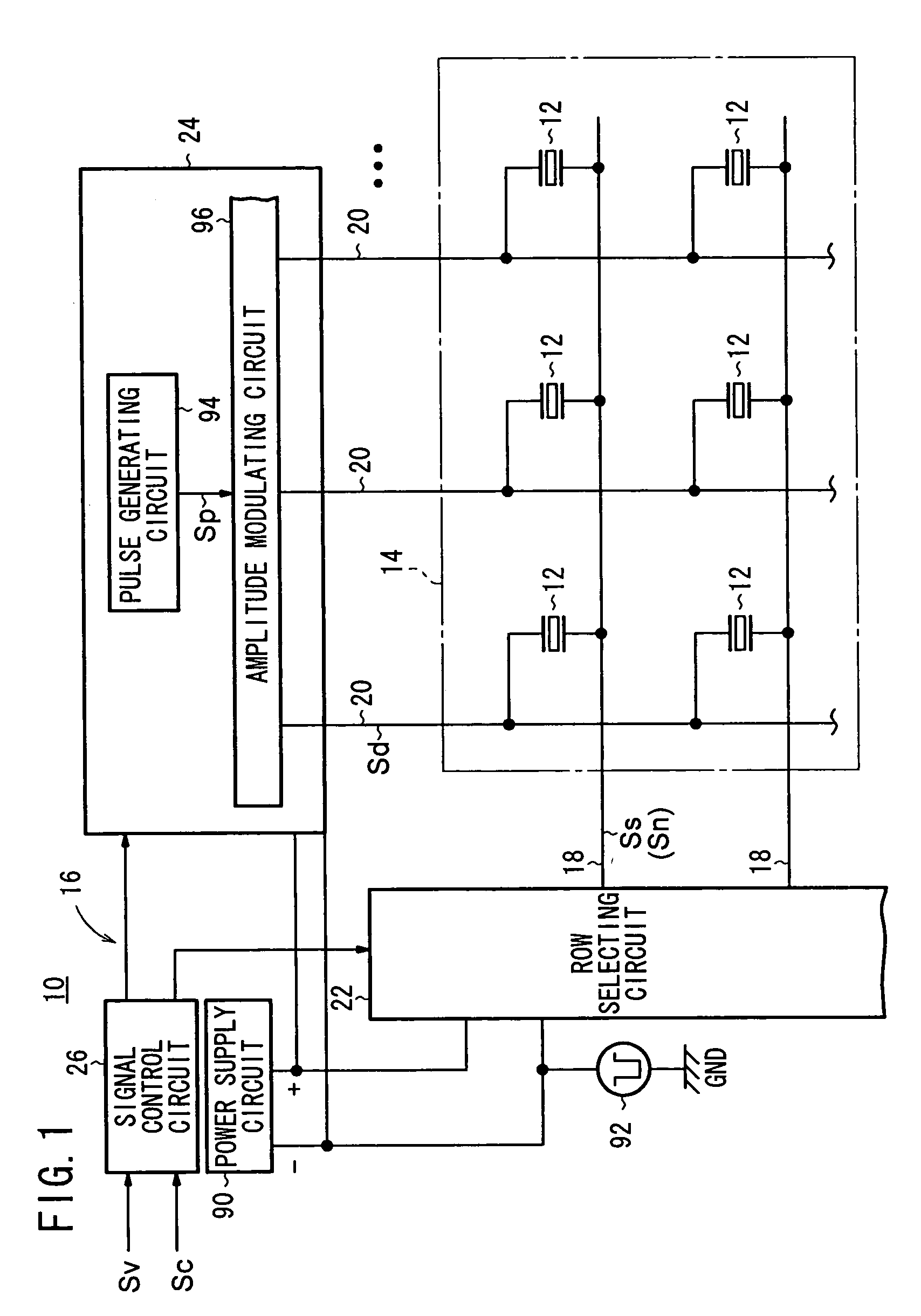
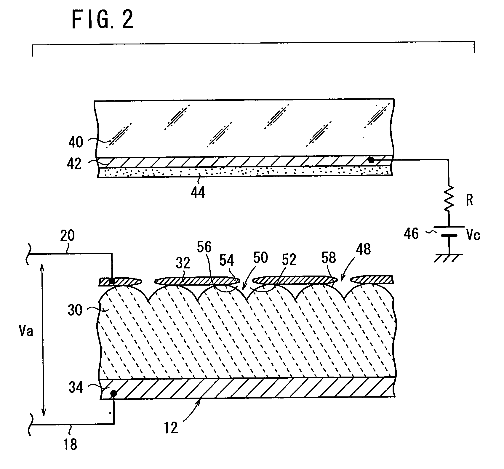
[0297] As shown in FIG. 33, a light source 10A according to the present invention has a transparent substrate 40, a fixed substrate 110 disposed in facing relation to the transparent substrate 40, and a plurality of electron emitters 12 disposed on a principal surface of the fixed substrate 110 which confronts the transparent substrate 40.

[0298] A spreading electrode 150 is disposed on a portion of the principal surface of the fixed substrate 110 which is free of the electron emitters 12. A phosphor layer 44 is disposed substantially entirely on the reverse side of the transparent substrate 40 which confronts the fixed substrate 110, and an anode electrode 42 which comprises a metal film is disposed on the lower end face of the phosphor layer 44. The anode electrode 42 also functions as a metal back layer 152. The anode electrode 42 may be formed by sputtering or vacuum evaporation, or may be in the form of a metal foil applied to the phosphor layer 44. The metal film serving as the...

second embodiment

[0306] the light source 10B can be designed with increased freedom for generating an electric field for spreading the electron flow 146 while keeping a desired insulating distance between the spreading electrode 156 and the drive electrodes and interconnects of the electron emitters 12. The insulating distance may also be maintained by a separate insulating substrate such as of glass or the like disposed between the electron emitters 12 and the fixed substrate 110.

third embodiment

[0307] As shown in FIG. 37, a light source 10C according to the present invention has a transparent substrate 40, a fixed substrate 110 disposed in facing relation to the transparent substrate 40, and a plurality of electron emitters 12 disposed on the reverse side of the transparent substrate 40 which confronts the fixed substrate 110. A spreading electrode 150 in the form of a transparent electrode is disposed on a portion of the reverse side of the transparent substrate 40 which is free of the electron emitters 12.

[0308] An anode electrode 42 which comprises a light reflecting film 142, for example, is disposed substantially entirely on the principal surface of the fixed substrate 110 which confronts the transparent substrate 40, and a phosphor layer 44 is disposed on the upper end face of the anode electrode 42.

[0309] When electrons emitted from the electron emitters 12 impinge upon the phosphor layer 44 on the principal surface of the fixed substrate 110, the phosphor layer 44...


PUM


Abstract

A light source has a transparent substrate, a fixed substrate disposed in facing relation to the transparent substrate, at least one electron emitter disposed on the fixed substrate, a phosphor layer disposed on a surface of the transparent substrate which confronts the fixed substrate, and a trajectory deflector for deflecting the trajectory of a pulsed electron flow intermittently emitted from the electron emitter. The pulsed electron flow is deflected by the trajectory deflector to two-dimensionally scan a position of the phosphor layer which is irradiated with the pulsed electron flow for thereby spreading the pulsed electron flow.

Description

BACKGROUND OF THE INVENTION [0001] 1. Field of the Invention [0002] The present invention relates to a light source (including a planar light source) comprising electron emitters each for emitting electrons from an emitter by applying a drive voltage to electrodes on the emitter. [0003] 2. Description of the Related Art [0004] Recently, electron emitters having a drive electrode and a common electrode have been finding use in various applications such as field emission displays (FEDs) and backlight units. In an FED, a plurality of electron emitters are arranged in a two-dimensional array, and a plurality of phosphors are positioned in association with the respective electron emitters with a predetermined gap left therebetween. [0005] Conventional electron emitters are disclosed in Japanese Laid-Open Patent Publication No. 1-311533, Japanese Laid-Open Patent Publication No. 7-147131, Japanese Laid-Open Patent Publication No. 2000-285801, Japanese Patent Publication No. 46-20944, and ...

Claims


Application Information

Patent Timeline
IPC IPC(8): H01J63/04
CPCB82Y10/00H01J1/312H01J1/32H01J63/06H01J2201/3125
Inventor OHWADA, IWAOSHIMOGAWA, NATSUMIKAMEJI, TETSUYUKIGOTO, NAOKISHIKATA, ISAO
Owner NGK INSULATORS LTD
Why Eureka
Try Eureka