Front-wing cantilever for the conductive probe of electrical scanning probe microscopes

a technology of conductive probe and microscope, which is applied in the direction of mechanical measurement arrangement, mechanical roughness/irregularity measurement, instruments, etc., can solve the problems of inaccurate measurement of p-n junction width and the above problems, and achieve the effect of promoting analysis accuracy

Inactive Publication Date: 2006-09-28
GRELL FARMS +1
View PDF2 Cites 0 Cited by
  • Summary
  • Abstract
  • Description
  • Claims
  • Application Information

AI Technical Summary

Benefits of technology

[0011] The primary objective of the present invention is to provide a front-wing cantilever for the conductive probe of electrical scanning probe microscopes, which can inhibit the optical perturbation in electrical scanning probe microscopes and can obviously promote the analysis accuracy.

Problems solved by technology

Thus, P-N junction width measured thereby is inaccurate.
As the optical perturbation results from the optical absorption of material, the above problems will become more serious for narrow energy gap materials, such as Si1-xGex, GaAs, InP, etc.

Method used


Image

  • Front-wing cantilever for the conductive probe of electrical scanning probe microscopes
  • Front-wing cantilever for the conductive probe of electrical scanning probe microscopes
  • Front-wing cantilever for the conductive probe of electrical scanning probe microscopes

Examples


Embodiment Construction

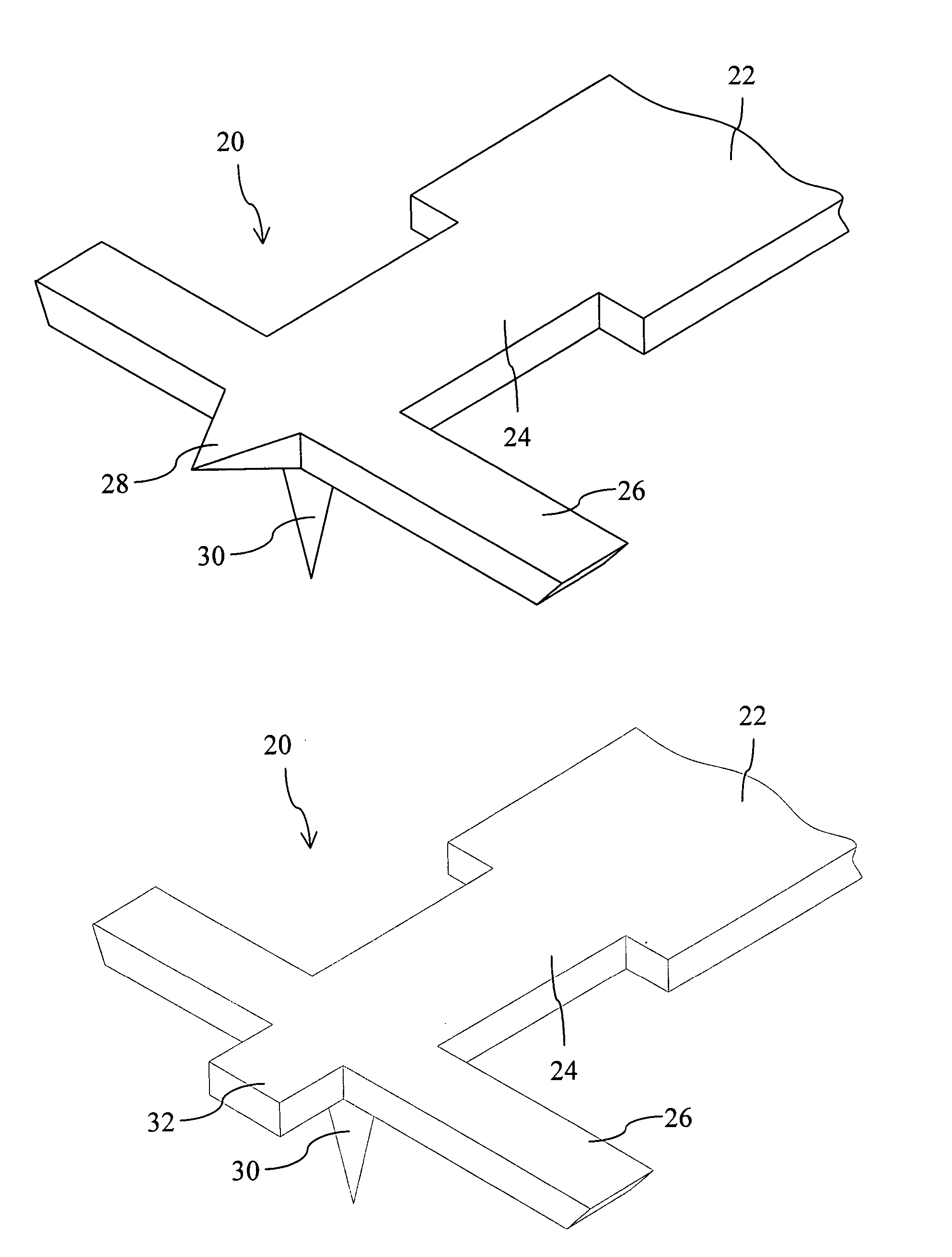
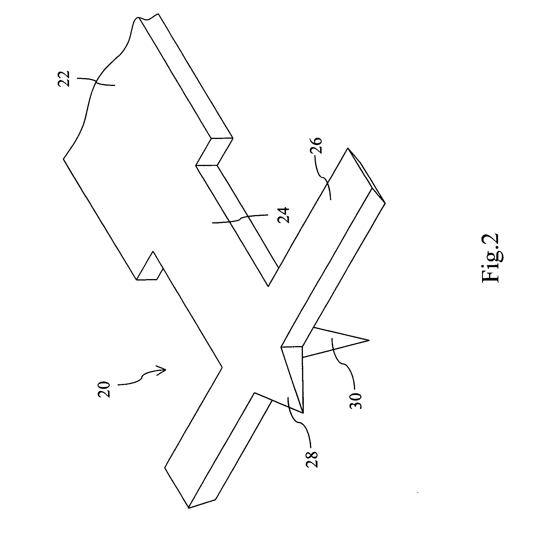
[0024] Herein, the present invention is to be exemplified by Scanning Capacitance Microscope (SCM); however, it is not intended to limit the scope of the present invention, and the application of the present invention to other Electrical Scanning Probe Microscopes, such as Scanning Spreading Resistance Microscopy (SSRM) and Conductive Atomic Force Microscopy (CAFM) are to be included within the scope of the present invention. The Scanning Capacitance Microscope primarily applies to the analysis of 2-dimensional distribution of carrier concentration and the measurement of the effective channel length of Metal Oxide Semiconductor (MOS) devices. However, the Scanning Capacitance Microscope is influenced by an optical perturbation, which brings about the increase in P-N junction measurement error and the decrease in image contrast. Owing to the above problems, when the Scanning Capacitance Microscope analyzes the carrier concentration distribution and the junction image within a nanomet...


PUM


Abstract

The present invention discloses a front-wing cantilever for the conductive probe of electrical scanning probe microscopes, wherein two symmetrical front wings are installed to extend from two lateral sides of the front end of the cantilever so that those two front wings are positioned on two lateral sides of the conductive tip. The front-wing structure of the cantilever can effectively inhibit the optical perturbation in the electrical scanning probe microscopes and obviously promote the analysis accuracy thereof. The front-wing structure can provide the scanned region with an effective dark field lest the optical absorption appears in the scanned region of semiconductor specimen and inhibit the optical perturbation occurs during the measurement and analysis of the differential capacitance.

Description

BACKGROUND OF THE INVENTION [0001] 1. Field of the Invention [0002] The present invention relates to electrical scanning probe microscopes, particularly to a front-wing cantilever for the conductive probe of electrical scanning probe microscopes, which can avoid the optical perturbation. [0003] 2. Description of the Related Art [0004] The Electrical Scanning Probe Microscopy (ESPM), which is a widely applied technology for surface electrical property analysis, has the characteristics of easy performance and can directly and rapidly provide the nanometric electrical information of material surface, such as the variations of current, resistance, and capacitance, and the information gained thereby has the advantage of high accuracy. Via the conductive probe's contacting the surface of specimen, various applications of Electrical Scanning Probe Microscopy can be evolved, such as Scanning Capacitance Microscopy (SCM), Scanning Spreading Resistance Microscopy (SSRM), and Conductive Atomic...

Claims


Application Information

Patent Timeline
Patent Type & Authority Applications(United States)
IPC IPC(8): G01R31/02
CPCB82Y35/00G01R1/06727G01R1/06711G01Q60/40
Inventor CHANG, MAO-NAN
Owner GRELL FARMS
Why Eureka
Try Eureka