Temperature compensation of thin film diode voltage threshold in memory sensing circuit

a technology of memory sensing circuit and temperature compensation, which is applied in the field of memory devices and diodes, can solve the problems of corresponding fluctuation of operation voltage levels reaching the nrm, and achieve the effect of constant operation voltage and constant operation voltag

Active Publication Date: 2006-09-28
CYPRESS SEMICON CORP
View PDF27 Cites 36 Cited by
  • Summary
  • Abstract
  • Description
  • Claims
  • Application Information

AI Technical Summary

Benefits of technology

[0013] Further, the subject invention includes a temperature sensitive bias circuit to provide a temperature compensating bias voltage to maintain a constant operation voltage across the NRM cell. The bias temperature sensitive bias circuit can include a thin film diode to track the threshold voltage fluctuations of the diode in the array core. The thin film diode can be in series with two resistors, which create a resistive ratio used to mimic the temperature effect on the NRM cell of the array core. The temperature sensitive bias circuit can generate a reference temperature compensating bias voltage. The generated voltage is duplicated by a differential amplifier to the NRM cell in order to maintain a constant operation voltage across the NRM cell. It is to be noted that the subject invention is not limited to the utilization of thi...

Problems solved by technology

Such variations can result in a corresponding fluc...

Method used


Image

  • Temperature compensation of thin film diode voltage threshold in memory sensing circuit
  • Temperature compensation of thin film diode voltage threshold in memory sensing circuit
  • Temperature compensation of thin film diode voltage threshold in memory sensing circuit

Examples


Embodiment Construction

[0024] The subject invention is now described with reference to the drawings, wherein like reference numerals are used to refer to like elements throughout. In the following description, for purposes of explanation, numerous specific details are set forth in order to provide a thorough understanding of the subject invention. It may be evident, however, that the subject invention may be practiced without these specific details. In other instances, well-known structures and devices are shown in block diagram form in order to facilitate describing the subject invention.

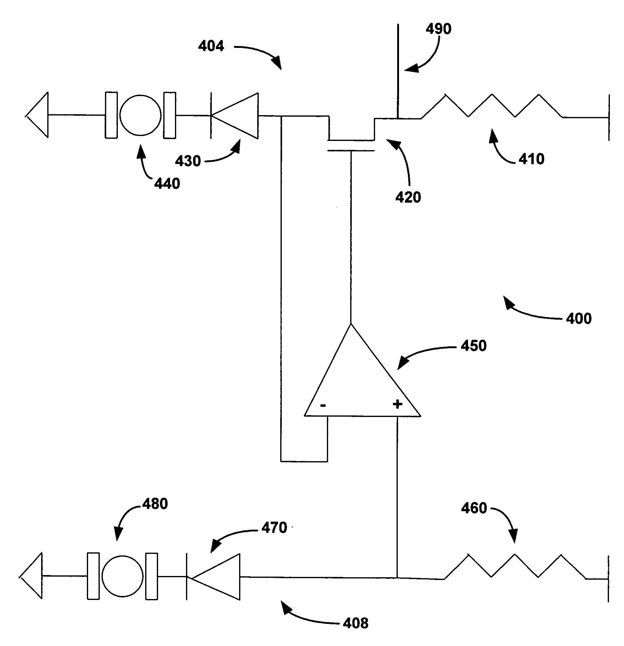
[0025] The subject invention provides for systems and methods of temperature compensation of thin film diode voltage levels in memory sensing circuits. A differential amplifier can be employed to duplicate a compensating bias reference voltage, generated by a temperature sensitive bias circuit, to a NRM cell in an array core and / or a memory array utilizing one or more temperature variable select devices. The array core,...


PUM


Abstract

Systems and methodologies are provided for temperature compensation of thin film diode voltage levels in memory sensing circuits. The subject invention includes a temperature sensitive bias circuit and an array core with a temperature variable select device. The array core can consist of a thin film diode in series with a nanoscale resistive memory cell. The temperature sensitive bias circuit can include a thin film diode in series with two resistors, and provides a temperature compensating bias voltage to the array core. The thin film diode of the temperature sensitive bias circuit tracks the diode of the array core, while the two resistors create a resistive ratio to mimic the effect of temperature and/or process variation(s) on the array core. The compensating bias reference voltage is generated by the temperature sensitive bias circuit, duplicated by a differential amplifier, and utilized to maintain a constant operation voltage level on the nanoscale resistive memory cell.

Description

TECHNICAL FIELD [0001] The subject invention generally relates to memory devices and diodes for selecting memory cells in memory arrays. In particular, the subject invention relates to memory devices containing controllably conductive layer(s). BACKGROUND ART [0002] The basic functions of a computer and memory devices include information processing and storage. In typical computer systems, these arithmetic, logic, and memory operations are performed by devices that are capable of reversibly switching between two states often referred to as “0” and “1.” Such switching devices are fabricated from semiconducting devices that perform these various functions and are capable of switching between two states at high speed. [0003] Electronic addressing or logic devices, for instance for storage or processing of data, are made with inorganic solid state technology, and particularly crystalline silicon devices. The metal oxide semiconductor field effect transistor (MOSFET) is one the main work...

Claims


Application Information

Patent Timeline
IPC IPC(8): G11C11/00
CPCB82Y10/00G11C7/04G11C11/5664G11C13/00G11C13/0014G11C13/0016G11C2213/72Y10S977/943
Inventor BILL, COLIN S.CAI, WEI DAISY
Owner CYPRESS SEMICON CORP
Why Eureka
Try Eureka