Light emitting device and its manufacturing method

a technology of light emitting device and manufacturing method, which is applied in the direction of solid-state devices, electric lighting sources, electric lighting sources, etc., can solve the problems of limited display range, difficult to form on glass or plastic substrates, and difficult to meet the requirements of lighting uniformity, etc., to achieve excellent luminous uniformity, low voltage, and drive stably

Inactive Publication Date: 2006-10-05
CANON KK
View PDF13 Cites 6 Cited by
  • Summary
  • Abstract
  • Description
  • Claims
  • Application Information

AI Technical Summary

Benefits of technology

[0009] According to the present invention, it is possible to provide a light emitting device which is excellent in luminous uniformity at the luminous surface, and can be driven stably under a relatively low voltage. Since, the light emitting device of the present invention is excellent in luminous uniformity at the luminous surface, and can be driven stably under a relatively low voltage, it is possible to utilize it for a display, a printing apparatus or a lighting apparatus.

Problems solved by technology

However, since it is produced by a process using crystal growth requiring high temperature, it is difficult to be formed on a glass substrate or a plastic substrate.
Thereby, the applicable range of a display is limited.
The organic EL display can be driven at a low voltage, and can be formed on a glass substrate or a plastic substrate, however, it has a problem in reliability or durability.
In the inorganic EL display, a large area of display can be relatively easily produced, and high environmental resistance during usage can be expected, however, as it is now, there is a problem of high driving voltage.

Method used


Image

  • Light emitting device and its manufacturing method
  • Light emitting device and its manufacturing method
  • Light emitting device and its manufacturing method

Examples


example 1

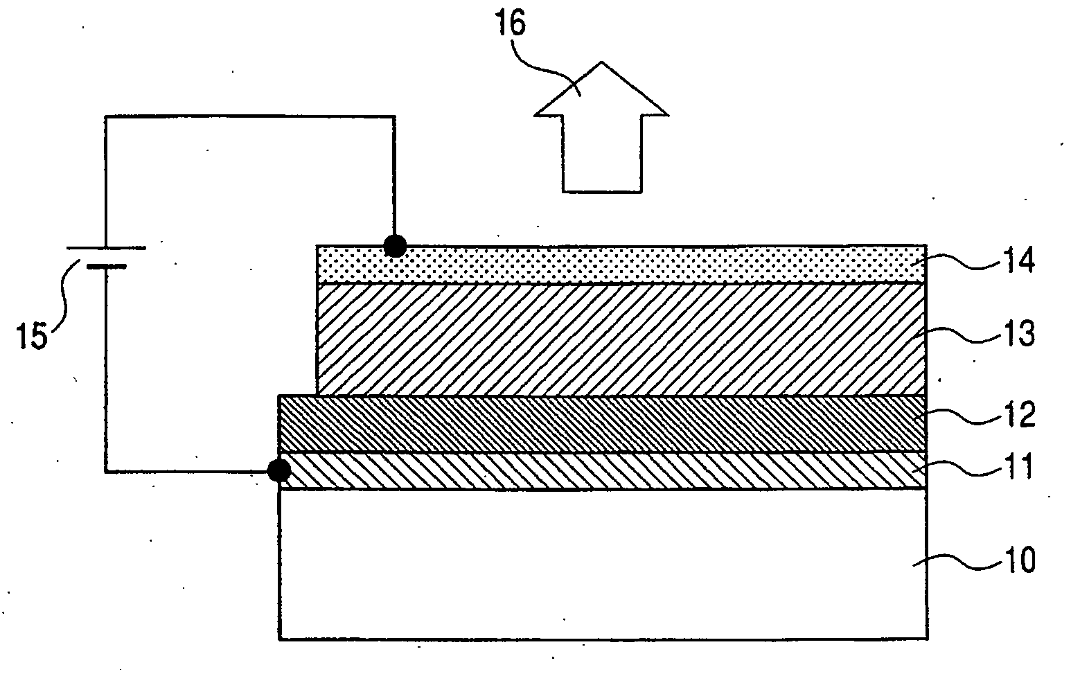
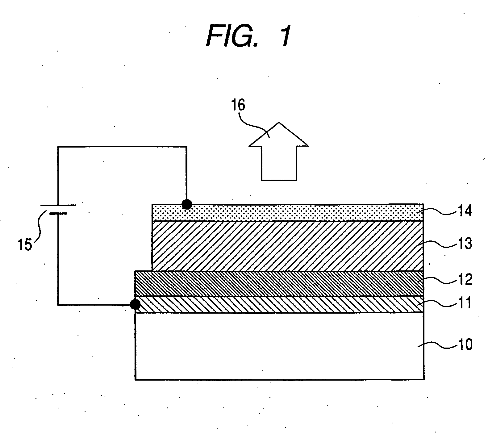
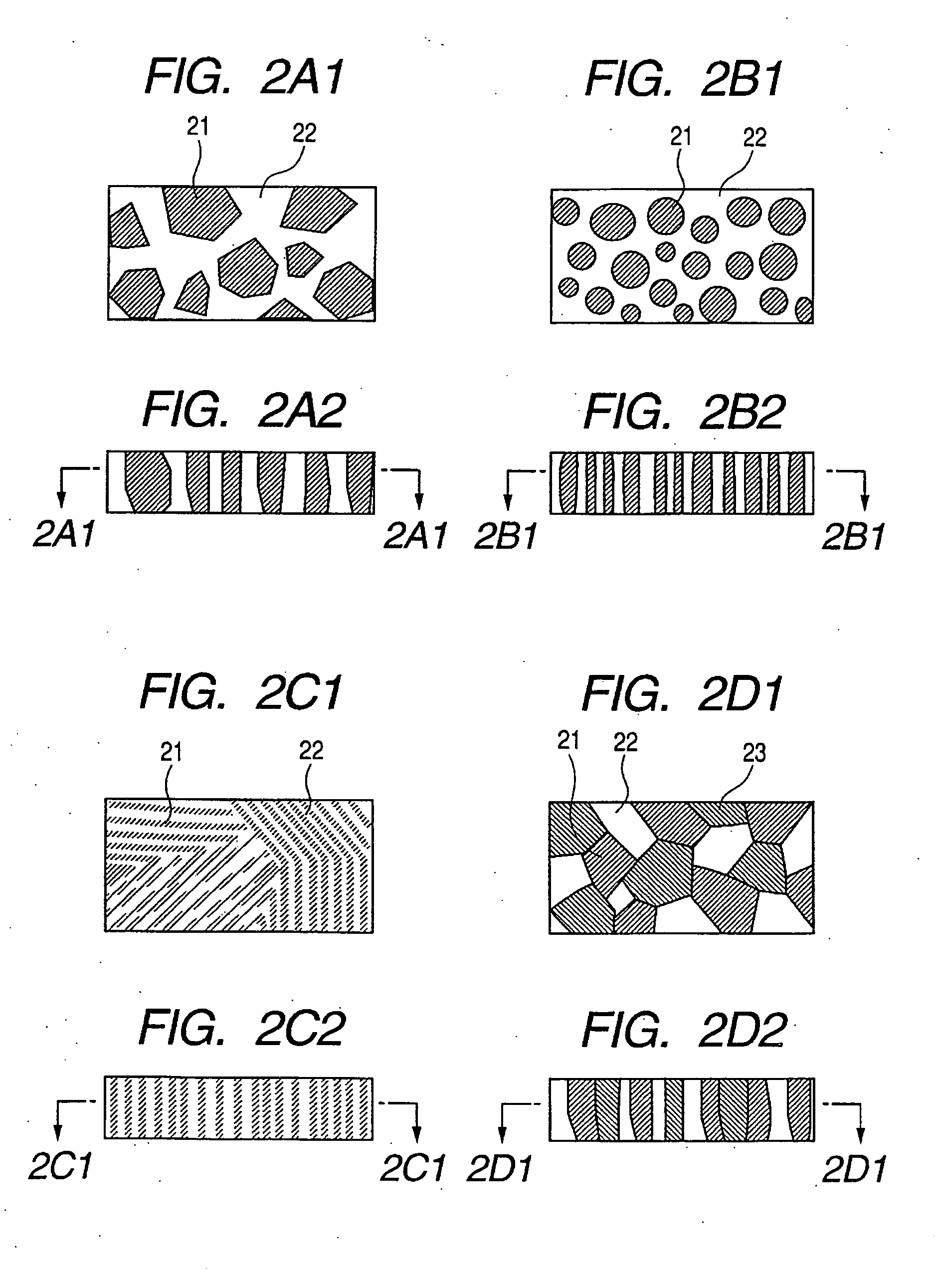
[0065] The light emitting device of this example comprises the structure described in FIG. 1. Microstructured layer 12 has the structure shown in FIG. 2B1 and 2B2, the first material is based on alumina, and the second material is based on silicon oxide.

[0066] Now, description will be made following the production steps.

[Formation of a First Electrode Layer]

[0067] A quartz substrate is prepared as a substrate 10. As a first material electrode layer 11, a Ta film with a thickness of 100 nm is formed on substrate 10 by a magnetron sputtering method.

[Formation of a Microstructured Layer]

[0068] A film of Al—Si matrix was formed on the first electrode layer at room temperature by a magnetron sputtering method. A target having a Al and Si composition ratio of (56:44) was used and an input power is 150 W. The Al—Si matrix comprises a matrix-structure, in which circular cylindrical columnar aluminum domains with a sectional diameter of about 7 nm are embedded in a matrix composed of Si...

example 2

[0071] The light emitting device of the present invention comprises the structure described in FIG. 4B. Microstructured layer 12 has the structure shown in FIGS. 2B1 and 2B2, and its first material is based on iron oxide, and its second material is based on silicon oxide.

[0072] Now, description will be made following the production steps.

[Formation of a Transparent Electrode Layer]

[0073] As substrate 10, a quartz substrate was used. An ITO film with a thickness of 200 nm was formed on substrate 10 by a magnetron sputtering method as a transparent electrode layer 14.

[Formation of a Microstructured Layer]

[0074] Next, a microstructured layer is formed on the transparent electrode layer 14 by a magnetron sputtering method, in which the target composed of a mixture of FeO powder and SiO2 powder with a volume ratio, FeO:SiO2=3:7 is used.

[0075] Next, the obtained structure is subjected to a heat treatment at 600° C. under an air atmosphere.

[0076] Thereby, the microstructured layer 1...

example 3

[0079] The light emitting device of the present invention comprises a structure described in FIG. 5. Reference numeral 17 denotes a third electrode layer, reference numeral 15a denotes a drive power supply, and reference numeral 15b denotes a second power supply. Electrons accelerated between the first electrode layer 11 and third electrode layer 17 are transmitted through the third electrode layer and injected into light emitting layer 13. Thus, the light emission layer is excited, thereby, light emission occurs.

[Formation of a First Electrode Layer and a Microstructured Layer]

[0080] A first electrode layer 11 and a microstructured layer 12 are formed on substrate 10, in a similar manner as in example 1.

[Formation of a Third Electrode Layer]

[0081] Next, as a third electrode layer 17, an Al film or an Au film with a thickness of 5 nm order is formed. In order to be transmitted by electrons, it is preferable for the layer to be thin as long as it acts as an electrode.

[Formation...


PUM


Abstract

The present invention is intended to provide a light emitting device which can be operated at a low voltage, has excellent luminous efficiency, stability, production cost, and the like. A light emitting device which has at least electrode layers 11, 14, a light emitting layer 13, a structure layer 12 between the electrode layer 11 and light emitting layer 13, wherein structure layer 12 has domains composed of a first material, and domains composed of a second material. It is preferable for the structure layer to have a plurality of columnar domains composed of the first material, and the domains composed of the second material around the domains composed of the first material, and for the domains composed of the first material are arranged regularly. It is preferable that the first material and the second material are composed of different oxides.

Description

BACKGROUND OF THE INVENTION [0001] 1. Field of the Invention [0002] The present invention relates to a light emitting device with an electrode layer, a light emitting layer and a microstructured layer, and its manufacturing method. [0003] 2. Related Background Art [0004] A flat panel display (FPD) to which a light emitting device is applied, has been drawing attention. From the type of a light emitting device applied thereto, FPD is classified into an organic electroluminescence display (organic EL display), an inorganic electroluminescence display (inorganic EL display), a light emitting diode display (LED display), or the like. [0005] LED can be driven under a low voltage, and is excellent in stability. However, since it is produced by a process using crystal growth requiring high temperature, it is difficult to be formed on a glass substrate or a plastic substrate. Thereby, the applicable range of a display is limited. [0006] The organic EL display can be driven at a low voltage,...

Claims


Application Information

Patent Timeline
Patent Type & Authority Applications(United States)
IPC IPC(8): H01L33/00B82Y20/00H01L51/50H05B33/10H05B33/14H05B33/22
CPCH01L33/16H01L33/18H01L51/5092H01L2924/0002H01L2924/00H10K50/171
Inventor IWASAKI, TATSUYADEN, TORU
Owner CANON KK
Why Eureka
Try Eureka