Mounting structure of double-path chip resistor

a chip resistor and mounting structure technology, applied in the field of chip resistors, can solve problems such as dimensional errors, and achieve the effect of enhancing soldering strength

Inactive Publication Date: 2006-10-05
ROHM CO LTD
View PDF2 Cites 7 Cited by
  • Summary
  • Abstract
  • Description
  • Claims
  • Application Information

AI Technical Summary

Benefits of technology

[0025] Preferably, the pitch interval between the two resistor elements may be substantially equal to the pitch interval of the land patterns. In this mann

Problems solved by technology

Such dimensional errors can be generated due to the manufacturing process where a large mater

Method used


Image

  • Mounting structure of double-path chip resistor
  • Mounting structure of double-path chip resistor
  • Mounting structure of double-path chip resistor

Examples


Embodiment Construction

[0036] A preferred embodiment of the present invention will be described below with reference to FIGS. 8-9.

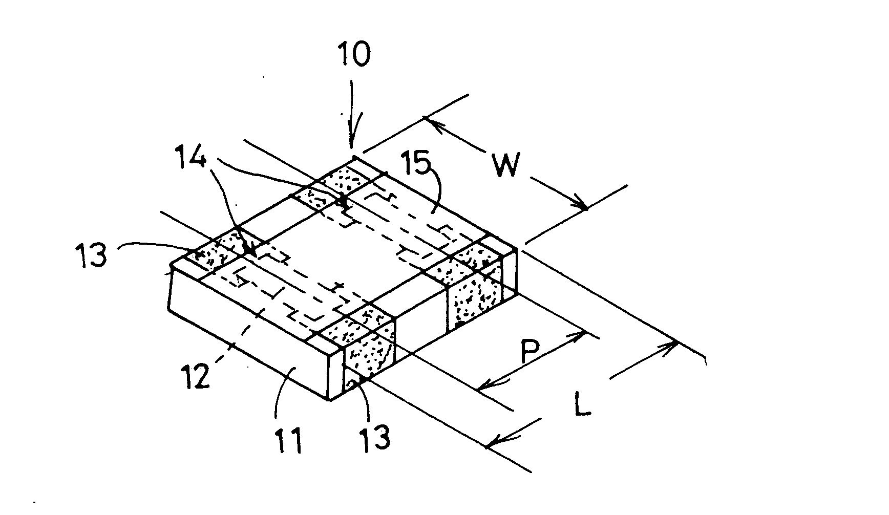
[0037]FIG. 8 illustrates a dual-element chip resistor 10 according to the present invention.

[0038] The dual-element chip resistor 10 comprises single chip-type insulating substrate 11 which is rectangular in plan view, and also comprises two parallel-arranged resistor elements 14 each of which is made of a resistor film 12 formed on the substrate 11, and terminal electrodes 13 at the both ends of the substrate. The chip resistor 10 further comprises a protective film 15 covering the resistor films 12 of the resistor elements 14.

[0039] The insulating substrate 11 of the dual-element chip resistor 10 includes edges whose dimensions are determined as follows. The dimension L, which defines the length of an edge passing by both of the resistor elements 14, is set at L=0.7 mm which is 0.1 mm smaller than the double of the pitch interval P0 of the land patterns C constituting the ...


PUM


Abstract

A mounting structure includes a printed circuit board and a dual-element chip resistor fixed to the circuit board. The chip resistor includes a rectangular insulating substrate and two resistor elements arranged in parallel to each other on the circuit board. Each resistor element includes an elongated resistor film formed on the substrate and two terminal electrodes at respective ends of the resistor film. The circuit board has a surface provided with at least four land patterns disposed with a predetermined pitch. The chip resistor is soldered to adjacent two of these four land patterns. The substrate of the chip resistor includes an edge extending in a direction in which the two resistor elements are spaced away from each other, and the edge of the substrate has a length which is smaller than double the pitch interval of the land patterns.

Description

BACKGROUND OF THE INVENTION [0001] 1. Field of the Invention [0002] The present invention relates to a chip resistor of dual-path or dual-element type that comprises a single rectangular insulating substrate, two parallel-arranged resistor elements each made of a resistor film formed on the substrate, and terminal electrodes at the both ends of the substrate. In particular, the present invention relates to a mounting structure for mounting and soldering such a dual-path-chip resistor on a printed circuit board. [0003] 2. Description of the Related Art [0004] Widely known chip resistors include a chip resistor comprising one resistor element (hereinafter, referred to as “single-element chip resistor”) A1 as shown in FIG. 1, a chip resistor comprising two resistor elements (hereinafter, referred to as “dual-element chip resistor”) A2 as shown in FIG. 2, and a chip resistor comprising four resistor elements (hereinafter, referred to as “quad-element chip resistor”) A4 as shown in FIG. ...

Claims


Application Information

Patent Timeline
IPC IPC(8): H01C1/012
CPCH01C1/012H05K2201/10636H05K3/3442H05K1/181Y02P70/50H01C1/01
Inventor KURIYAMA, TAKAHIRO
Owner ROHM CO LTD
Why Eureka
Try Eureka