Plasma display panel and plasma display device

a display panel and plasma technology, applied in the direction of static indicating devices, address electrodes, instruments, etc., can solve the problems of increased cost of driving circuits, and achieve the effect of reducing the voltage for generating the address discharge and improving the luminan

Inactive Publication Date: 2006-10-05
FUJITSU HITACHI PLASMA DISPLAY LTD
View PDF0 Cites 3 Cited by
  • Summary
  • Abstract
  • Description
  • Claims
  • Application Information

AI Technical Summary

Benefits of technology

[0026] The discharge gas contains at least neon (Ne) and xenon (Xe), and the mixing ratio of xenon is desirably 10 percent or more. Consequently, luminance can be improved. In addition, since the fourth (address) electrode is formed on the first substrate on which the second (Y) electrode is also formed, the voltage for generating the address discharge can be reduced.

Problems solved by technology

Therefore, since the driving circuits of the Y electrodes and the address electrodes have to output high voltages, a problem that the cost of the driving circuits is increased occurs.

Method used


Image

  • Plasma display panel and plasma display device
  • Plasma display panel and plasma display device
  • Plasma display panel and plasma display device

Examples


second embodiment

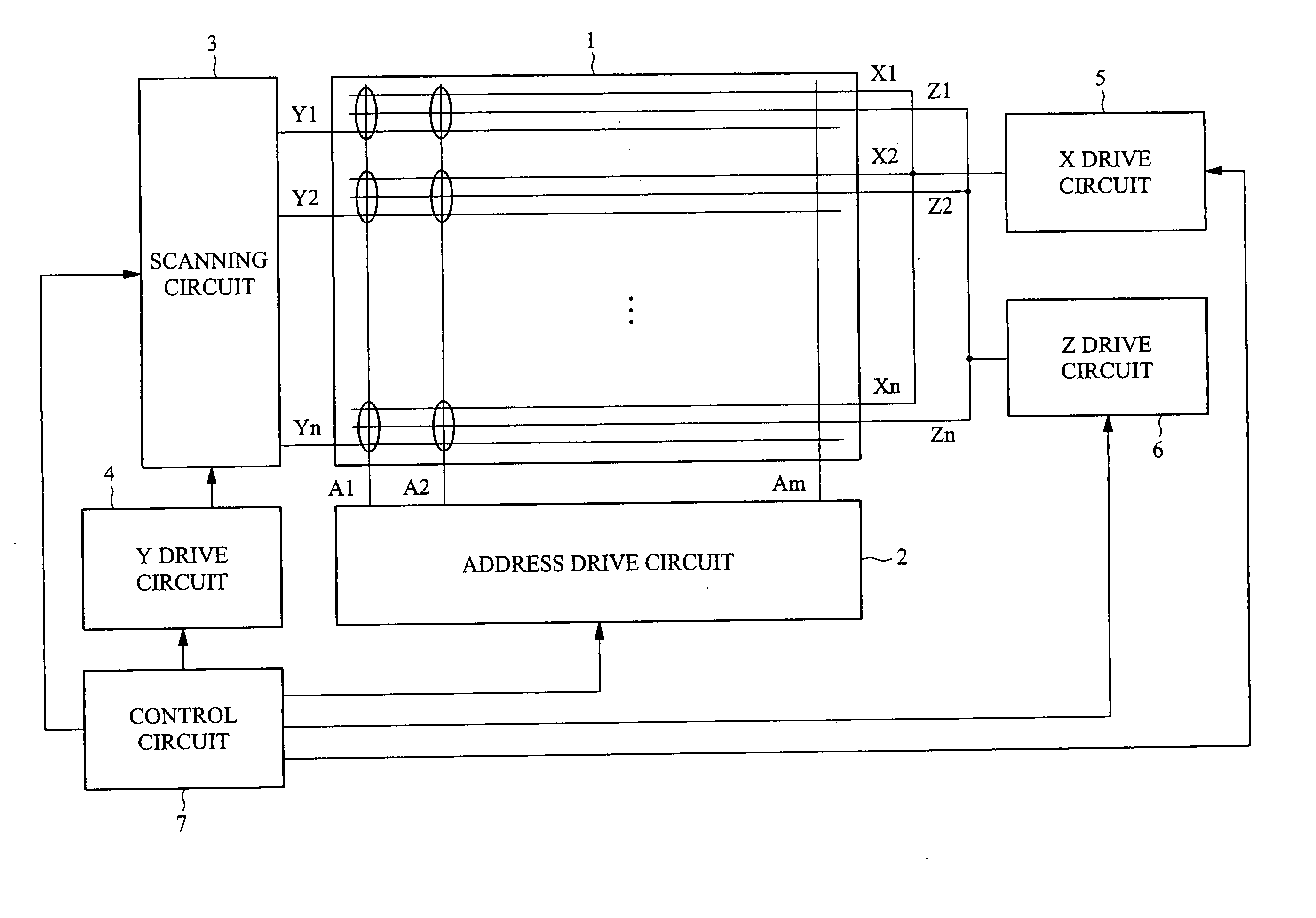
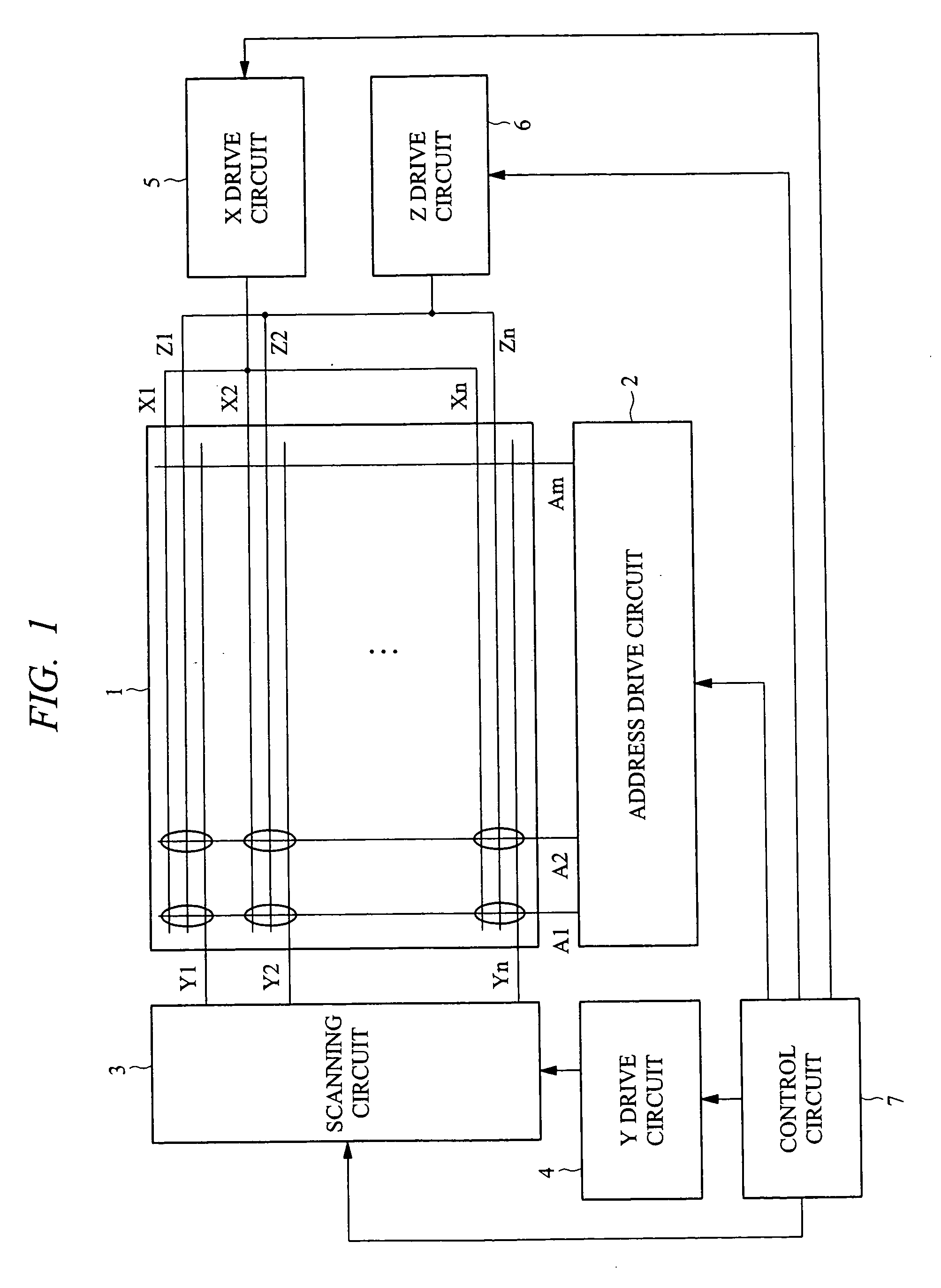
[0079]FIG. 11 is a diagram showing the entire structure of a PDP device of the second embodiment of the present invention. The second embodiment is an example in which the present invention is applied to an ALIS-type PDP device disclosed in Patent Document 3. The PDP 1 of the second embodiment is different from the PDP of the first embodiment in that the third electrodes (Z electrodes) are provided between all of the first (X) electrodes and the second (Y) electrodes, and all the spaces between the first (X) electrodes and the second (Y) electrodes are utilized as display lines. Since the ALIS method is disclosed in Patent Document 3, detailed description thereof will be omitted here.

[0080] As shown in FIG. 11, the plasma display panel 1 has a plurality of laterally (longitudinally) extending first electrodes (X electrodes) and second electrodes (Y electrodes). The plurality of X electrodes and Y electrodes are alternately disposed, and the number of the lines of the X electrodes i...


PUM


Abstract

A plasma display panel in which firing voltages between any of electrodes are low can be realized. A plasma display panel has a first substrate and a second substrate. The first substrate has a group of laterally extending first electrodes for performing sustain discharge and a group of laterally extending second electrodes which can be independently driven, a group of third electrodes positioned between the first and second electrodes, a dielectric layer covering-them, a group of fourth electrodes extending vertically and provided on the dielectric layer, and a protective layer. The second substrate has barrier ribs provided in parallel to the fourth electrodes so as to divide at least the first to third electrodes in the extending directions, and phosphors for emitting light when excited by an ultraviolet ray.

Description

CROSS-REFERENCE TO RELATED APPLICATION [0001] The present application claims priority from Japanese Patent Application No. JP 2005-101331 filed on Mar. 31, 2005, the content of which is hereby incorporated by reference into this application. TECHNICAL FIELD OF THE INVENTION [0002] The present invention relates to an A / C plasma display panel (PDP) and a plasma display device (PDP device) used for a display device of a personal computer and a workstation, a flat TV, and a plasma display for displaying advertisements, information, and others. BACKGROUND OF THE INVENTION [0003] In AC color PDP devices, an address / display separation (ADS) method in which a period when the cells to be displayed are determined (address period) and a display period when discharges for display lighting are performed (sustain discharge period) are separated has been widely employed. In this method, charge is accumulated in the cells, which are to be lit, in the address period, and discharges for display are p...

Claims


Application Information

Patent Timeline
Patent Type & Authority Applications(United States)
IPC IPC(8): G09G3/28G09G3/20G09G3/288G09G3/291G09G3/292G09G3/293G09G3/294G09G3/296G09G3/298G09G3/299H01J11/14H01J11/22H01J11/24H01J11/26H01J11/34H01J11/38H01J11/50
CPCG09G3/294G09G3/2986G09G3/299H01J2211/363H01J11/24H01J11/36H01J2211/245H01J11/12G09G3/291H01J11/22H01J11/34
Inventor SASAKI, TAKASHIKOBAYASHI, TAKAYUKIITOKAWA, NAOKIOTSUKA, AKIRA
Owner FUJITSU HITACHI PLASMA DISPLAY LTD
Why Eureka
Try Eureka