PCB solder masking process

a solder masking and pcb technology, applied in the direction of circuit masks, soldering apparatus, non-printed masks, etc., can solve the problems of increased investment and production costs, monotonous solder masking structure color, and lack of change, so as to achieve lower production costs and higher pcb quality

Inactive Publication Date: 2006-10-12
YANG HO CHING
View PDF9 Cites 5 Cited by
  • Summary
  • Abstract
  • Description
  • Claims
  • Application Information

AI Technical Summary

Benefits of technology

[0011] The primary purpose of the present invention is to provide a PCB solder masking process that corrects the flaws found with the process of the prior art, and allows lower production cost and higher PCB quality.

Problems solved by technology

Higher production cost since more consumption items and longer process time are required; 2.
Increased investment and production costs in the comparatively advanced facilities to achieve the purpose of consistently dispensed ink; 4.
Significant variation in dimension resulted from the relative humidity to discourage production reliability, as the negative used is highly sensitive to the ambient temperature.
Furthermore, the color of the solder masking structure appears to be monotonous, lacking in change, and vulnerable to scratch.

Method used


Image

  • PCB solder masking process
  • PCB solder masking process
  • PCB solder masking process

Examples


Embodiment Construction

[0021] The following descriptions are of exemplary embodiments only, and are not intended to limit the scope, applicability or configuration of the invention in any way. Rather, the following description provides a convenient illustration for implementing exemplary embodiments of the invention. Various changes to the described embodiments may be made in the function and arrangement of the elements described without departing from the scope of the invention as set forth in the appended claims.

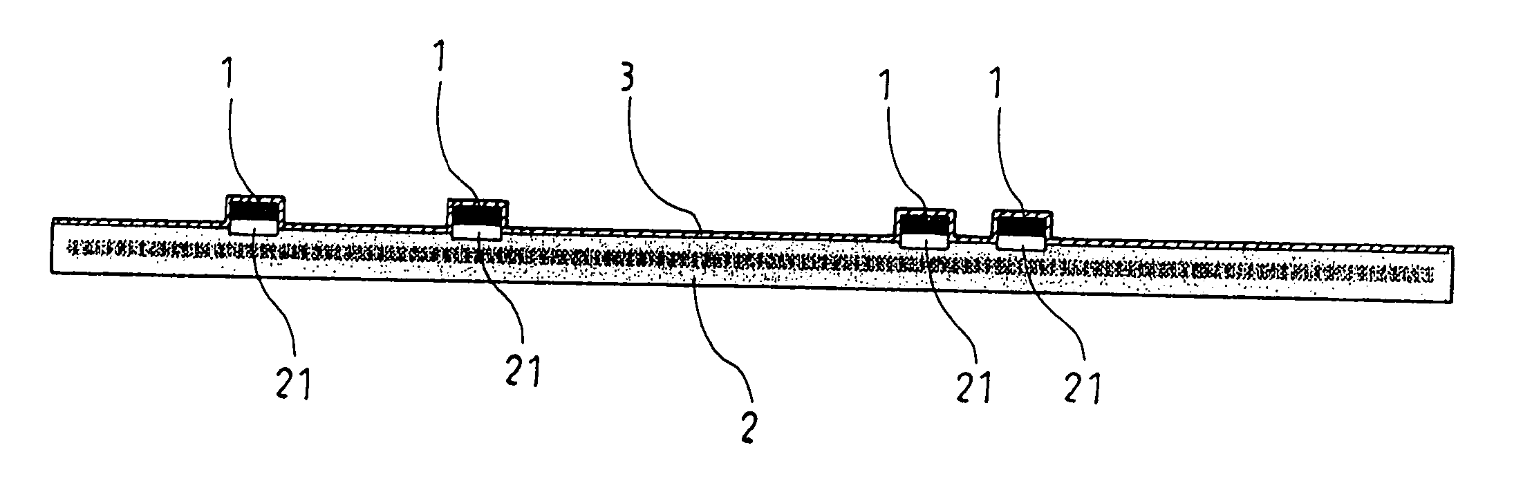
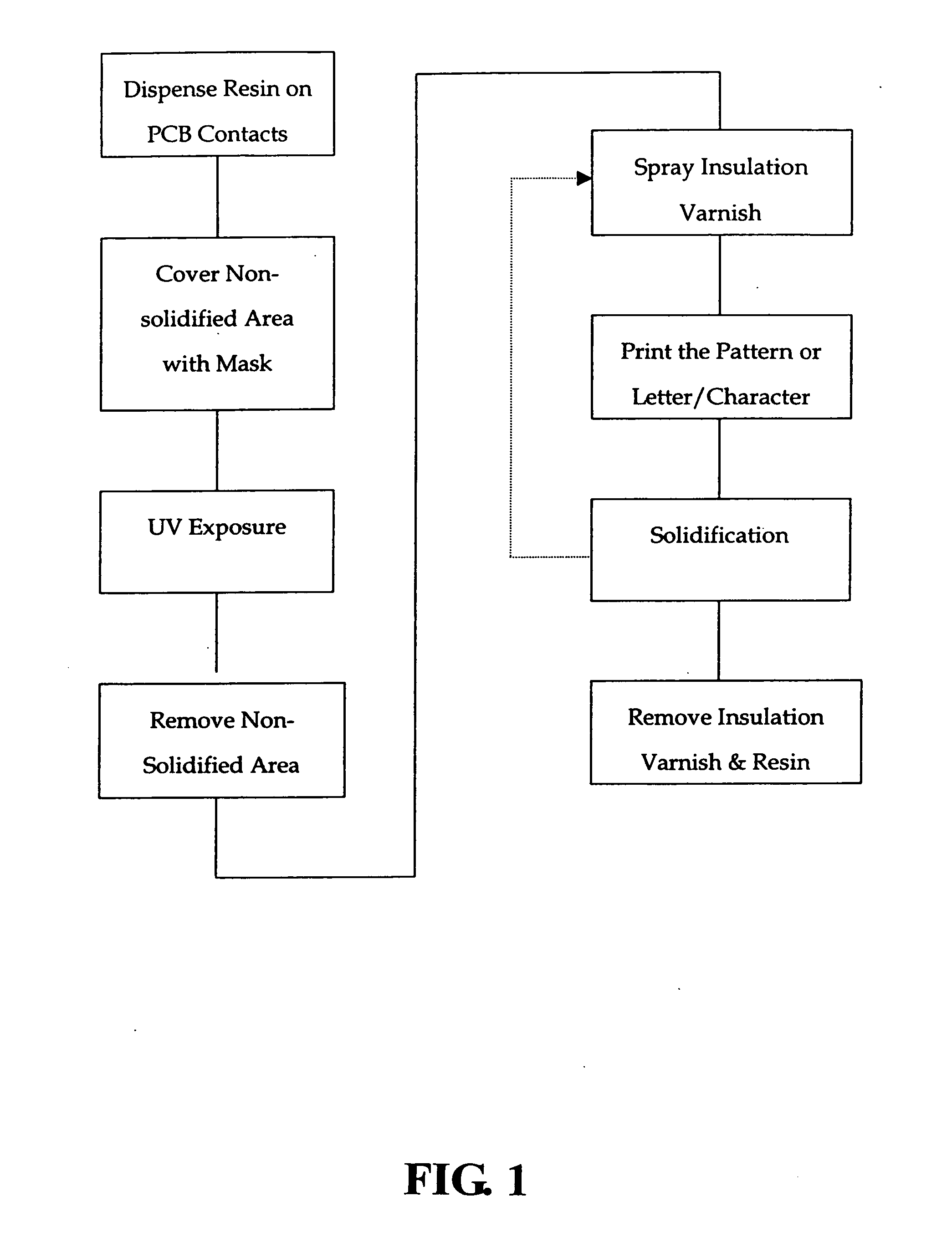
[0022] Referring to FIGS. 1 through 5, the solder masking process of the present invention is essentially comprised of the following steps:

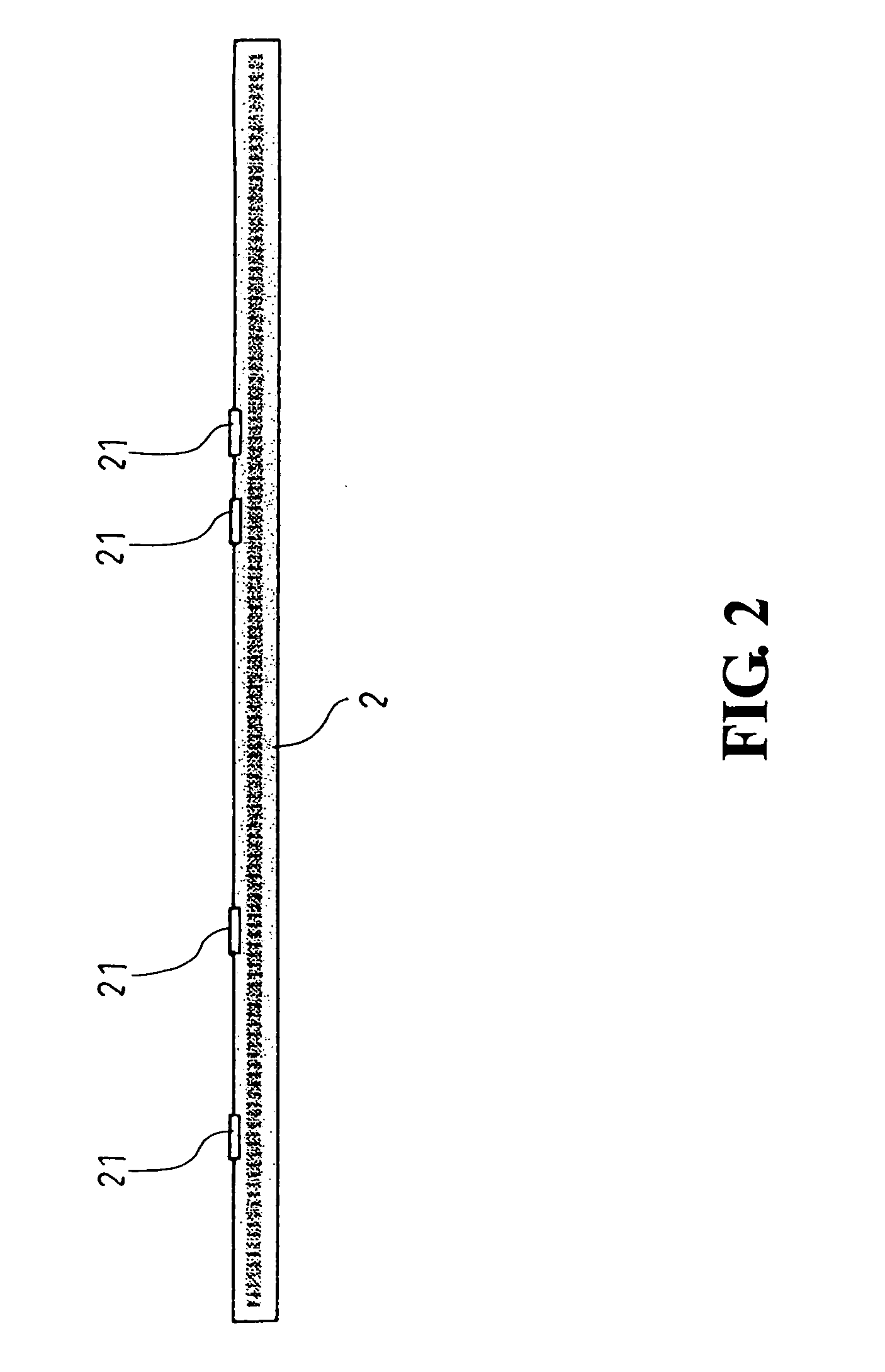
[0023] Step 1: a steel plate is produced by following a pattern as demanded and drilled with multiple holes at where a plurality of contacts 21 to be exposed from a PCB 2 and the diameter of each hole must be greater than that of the contact 21; each hole is dispensed with a resin 1 of a low hardness though the steel plate to such extent that the dispensed ...


PUM

PropertyMeasurementUnit
hardnessaaaaaaaaaa
areaaaaaaaaaaa
coloraaaaaaaaaa

Abstract

A PCB solder masking process allowing easier process, reduced production cost and improved PCB quality involves dispensing low hardness resin on contacts to be exposed on the PCB, resin being solidified, non-solidified area covered with mask, UV exposed, non-solidified area removed, PCB sprayed insulation varnish, solidified, varnish and resin on surface of contact removed, either sanded or sandblasted, and finally cleaned and rinsed.

Description

BACKGROUND OF THE INVENTION [0001] (a) Technical Field of the Invention [0002] The present invention is related to a PBC solder masking process, and more particularly, to one that is simple, low-cost, and capable of correcting variation in electric characteristics due to poor dispensing of solder masking material found in the prior art. [0003] (b) Description of the Prior Art [0004] Whereas the PCB solder masking process is usually done by having exposed the negative of the circuitry and made it into a screen, then ink printed to coat the screen on the area where exposed out of the contacts, the process is found with the following flaws: [0005] 1. Higher production cost since more consumption items and longer process time are required; [0006] 2. PCB electric characteristics are affected by variation in resistance due to inconsistent thickness of the ink dispensed; [0007] 3. Increased investment and production costs in the comparatively advanced facilities to achieve the purpose of c...

Claims


Application Information

Patent Timeline
Patent Type & Authority Applications(United States)
IPC IPC(8): B23K31/00
CPCB23K3/0607B23K2201/42H05K3/0044H05K3/0082H05K2203/0582H05K3/288H05K2203/025H05K2203/0557H05K3/28B23K2101/42
Inventor YANG, HO-CHING
Owner YANG HO CHING
Why Eureka
Try Eureka