Semiconductor device formed by using MEMS technique

a technology of mems and semiconductors, applied in the direction of relays, generators/motors, contacts, etc., can solve the problems of high power, increase in cost, and not suitable for portable devices

Inactive Publication Date: 2006-10-12
KK TOSHIBA
View PDF4 Cites 28 Cited by
  • Summary
  • Abstract
  • Description
  • Claims
  • Application Information

AI Technical Summary

Problems solved by technology

Of these schemes, the thermal type scheme and electromagnetic type scheme consume high power and hence are not suitable to be mounted in portable devices.
Since this voltage is higher than the power supply voltage of a cellular phone system, a component or circuit which generates a high voltage is required, resulting in an increase in cost.
In addition, as a high voltage is generated, the power consumption increases.
It is known that in an electrostatic type variable capacitor or switch, charge is trapped in the insulating film between electrodes owing to this high voltage.
However, as switching is repeated, a large amount of charge is stored, and the pull-out voltage shifts.
iv) In a MEMS variable capacitor, the adhesion between electrodes is poor (Even if the electrodes have minute recesses or warpage, strong driving force can bring the electrodes into tight contact with each other.
None of them are sufficient, are required to be improved.

Method used


Image

  • Semiconductor device formed by using MEMS technique
  • Semiconductor device formed by using MEMS technique
  • Semiconductor device formed by using MEMS technique

Examples


first embodiment

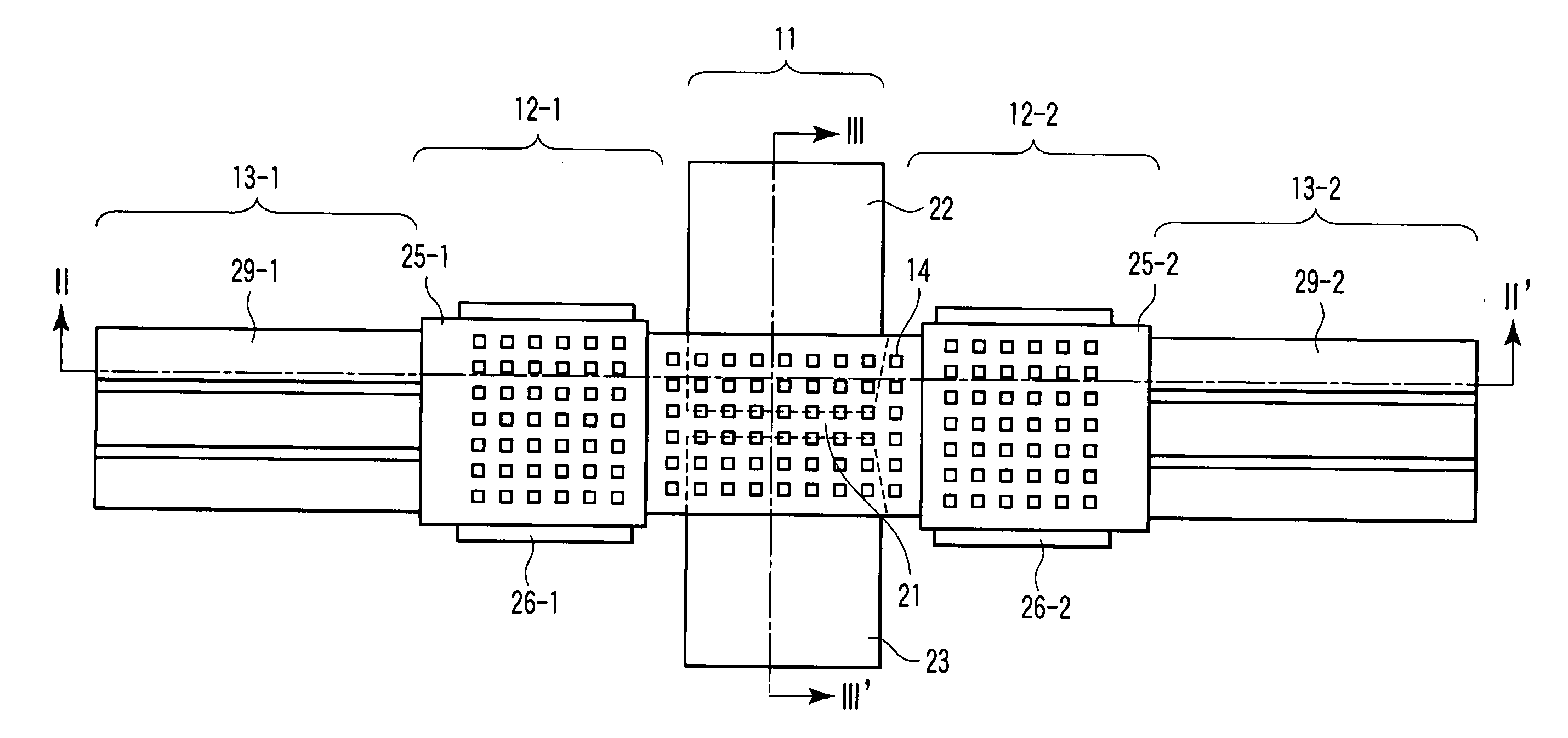
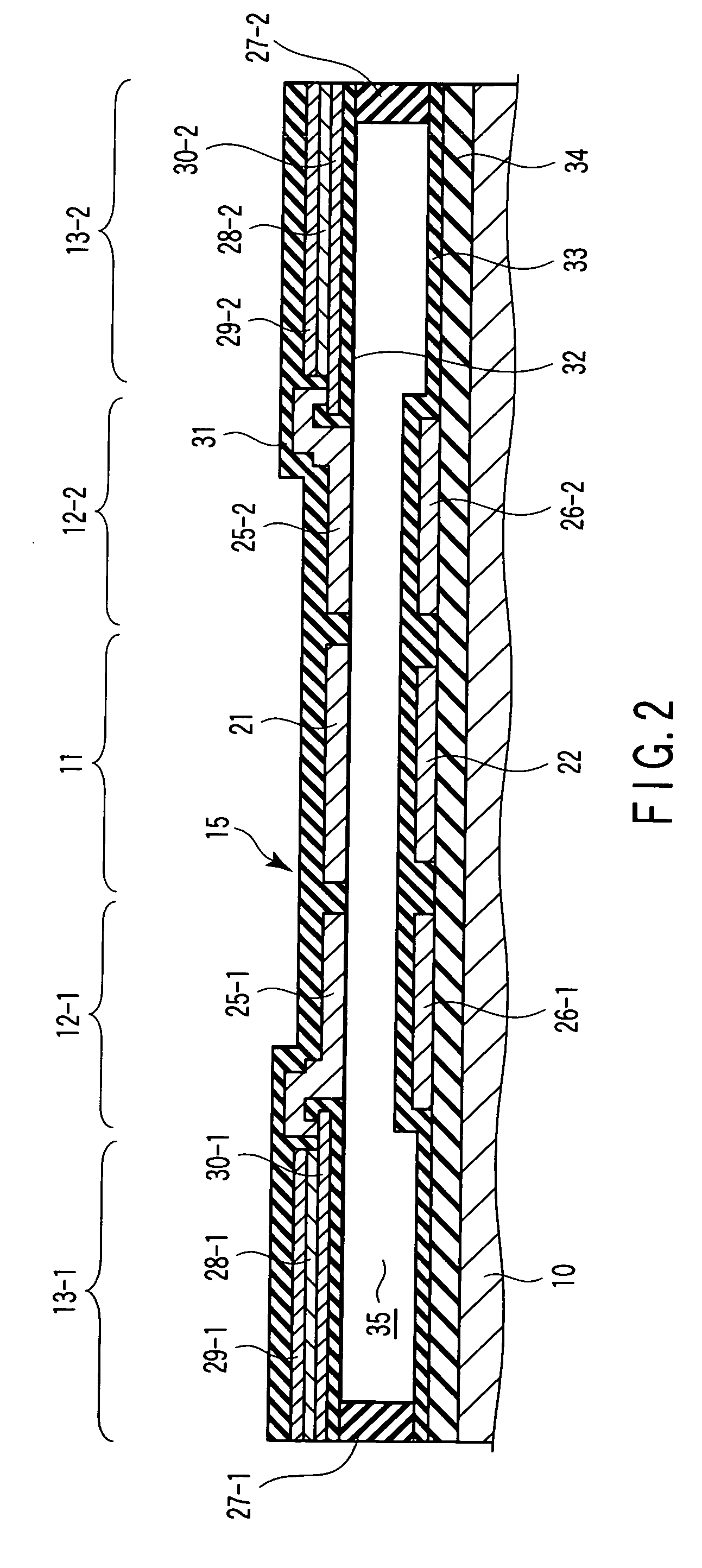
[0046] FIGS. 1 to 3 are views for explaining a semiconductor device according to the first embodiment of the present invention. FIG. 1 is a plan view of a variable capacitor. FIG. 2 is a sectional view taken along a line II-II′ in FIG. 1. FIG. 3 is a sectional view taken along a line III-III′ in FIG. 1. This semiconductor device comprises a variable capacitor unit 11, electrostatic actuator units 12-1 and 12-2, and piezoelectric actuator units 13-1 and 13-2. The piezoelectric actuator unit 13-1, electrostatic actuator unit 12-1, variable capacitor unit 11, electrostatic actuator unit 12-2, and piezoelectric actuator unit 13-2 are linearly arranged in one direction. These units are formed in a structure formed such that the two ends of an elastic member 15 are fixed on a substrate (e.g., a silicon substrate) 10 with anchors 27-1 and 27-2. A hollow 35 is formed between the elastic member 15 and the substrate 10. When the piezoelectric actuator units 13-1 and 13-2 and the electrostatic...

second embodiment

[0070]FIGS. 9 and 10 are views for explaining a semiconductor device according to the second embodiment of the present invention. FIG. 9 is a plan view of a variable capacitor. FIG. 10 is a sectional view taken along a line X-X′ in FIG. 9. A cross-section taken along a line III-III′ in FIG. 9 is the same as that in FIG. 3.

[0071] This semiconductor device comprises a variable capacitor unit 11, electrostatic actuator unit 12, and piezoelectric actuator unit 13. These units are formed in a structure formed such that one end of an elastic member 15 is fixed on a substrate (e.g., a silicon substrate) 10 with an anchor 27. A hollow 35′ is formed between the elastic member 15 and the substrate 10. When the piezoelectric actuator unit 13 and the electrostatic actuator unit 12 are driven, the other end (an upper electrode 21 of the variable capacitor unit 11) of the elastic member 15 deforms to move close to the substrate 10 (a lower electrode 22 of the variable capacitor unit 11), and the...

third embodiment

[0074]FIG. 11 is a view for explaining a semiconductor device according to the third embodiment of the present invention. FIG. 11 is a plan view of a variable capacitor. This semiconductor device comprises a variable capacitor unit 11, electrostatic actuator units 12-1 and 12-2, and piezoelectric actuator units 13-1, 13-2, 13-3, and 13-4. In the third embodiment, the variable capacitor unit, electrostatic actuator units, and piezoelectric actuator units are not arranged linearly, but the piezoelectric actuator units 13-1, 13-2, 13-3, and 13-4 are arranged nonlinearly. More specifically, the piezoelectric actuator units 13-1 and 13-3 are arranged on the opposite sides of the electrostatic actuator unit 12-1, and the piezoelectric actuator units 13-2 and 13-4 are arranged on the opposite side of the electrostatic actuator unit 12-2.

[0075] With such an arrangement as well, the device operates basically in the same manner as in the first embodiment, and substantially the same functions...


PUM


Abstract

A semiconductor device includes an elastic member, first and second electrodes, a piezoelectric actuator, and an electrostatic actuator. One end of the elastic member is fixed on a substrate through an anchor so as to form a gap between the elastic member and the substrate. The first and second electrodes are placed to face the other end of the elastic member and the substrate, respectively. The piezoelectric actuator deforms the other end of the elastic member to bring it close to the substrate. The electrostatic actuator includes a third electrode placed in the elastic member and a fourth electrode placed on the substrate so as to face the third electrode, and deforms the other end of the elastic member so as to bring it close to the substrate. The distance between the first and second electrodes is changed by driving the piezoelectric actuator and the electrostatic actuator.

Description

CROSS-REFERENCE TO RELATED APPLICATIONS [0001] This application is based upon and claims the benefit of priority from prior Japanese Patent Application No. 2005-113483, filed Apr. 11, 2005, the entire contents of which are incorporated herein by reference. BACKGROUND OF THE INVENTION [0002] 1. Field of the Invention [0003] The present invention relates to a semiconductor device such as a variable capacitor or switch formed by using a micromachining, or MEMS, (Micro-Electro-Mechanical Systems) technique. [0004] 2. Description of the Related Art [0005] A variable capacitor or switch manufactured by using the MEMS technique is advantageous over that using a PIN diode or FET in that, for example, the loss is small (the Q value is large) and distortion is small. Such devices are therefore expected to be mounted in next-generation cellular phones. [0006] As driving schemes for these MEMS variable capacitors and switches, an electrostatic type scheme, piezoelectric type scheme, thermal typ...

Claims


Application Information

Patent Timeline
Patent Type & Authority Applications(United States)
IPC IPC(8): H01L41/00B81B3/00H01G5/18H01L21/822H01L27/04H01L41/08H01L41/09H01L41/187
CPCH01G5/18H01H59/0009H01H2001/0063H01H2057/006H01L41/0946H02N1/006H01G5/16H01L41/094H01H2059/0018H10N30/2043H10N30/2042
Inventor IKEHASHI, TAMIO
Owner KK TOSHIBA
Why Eureka
Try Eureka