

Organic light emitting device
Active Publication Date: 2006-10-12
SAMSUNG DISPLAY CO LTD
View PDF4 Cites 38 Cited by
- Summary
- Abstract
- Description
- Claims
- Application Information
AI Technical Summary
Benefits of technology
[0009] In one embodiment of the present invention, an organic light emitting device (OLED) has increased life span and improved current injection properties due to smoothed hole injection and regulated electron injection.
Problems solved by technology
To lengthen the OLED's life span (which is the device's biggest disadvantage), it is necessary to prevent diffusion of oxygen, ions, or small molecules from the hole transport layer 122.
Method used
View moreImage
Smart ImageViewing Examples

Examples
example 1
[0052] A 1 nm thick C60 buffer layer was prepared for an OLED. A NPD hole transport layer was deposited in a vacuum. A 25 nm thick Alq3 organic emission layer was then deposited. An electron transport layer was formed on the organic emission layer. A 300 nm thick LiF / Al cathode was then deposited. Then, the OLED was encapsulated in a metal can with barium oxide.
example 2
[0053] An OLED was prepared as in Example 1, except that the buffer layer had a thickness of 3 nm.
example 3
[0054] An OLED was prepared as in Example 2, except that the buffer layer had a thickness of 5 nm.
Login to View More PUM
 Abstract
Organic light emitting devices are provided. One organic light emitting device includes a buffer layer including a fullerene-based material and a hole injection layer and / or a hole transport layer doped with the fullerene-based material.
Description
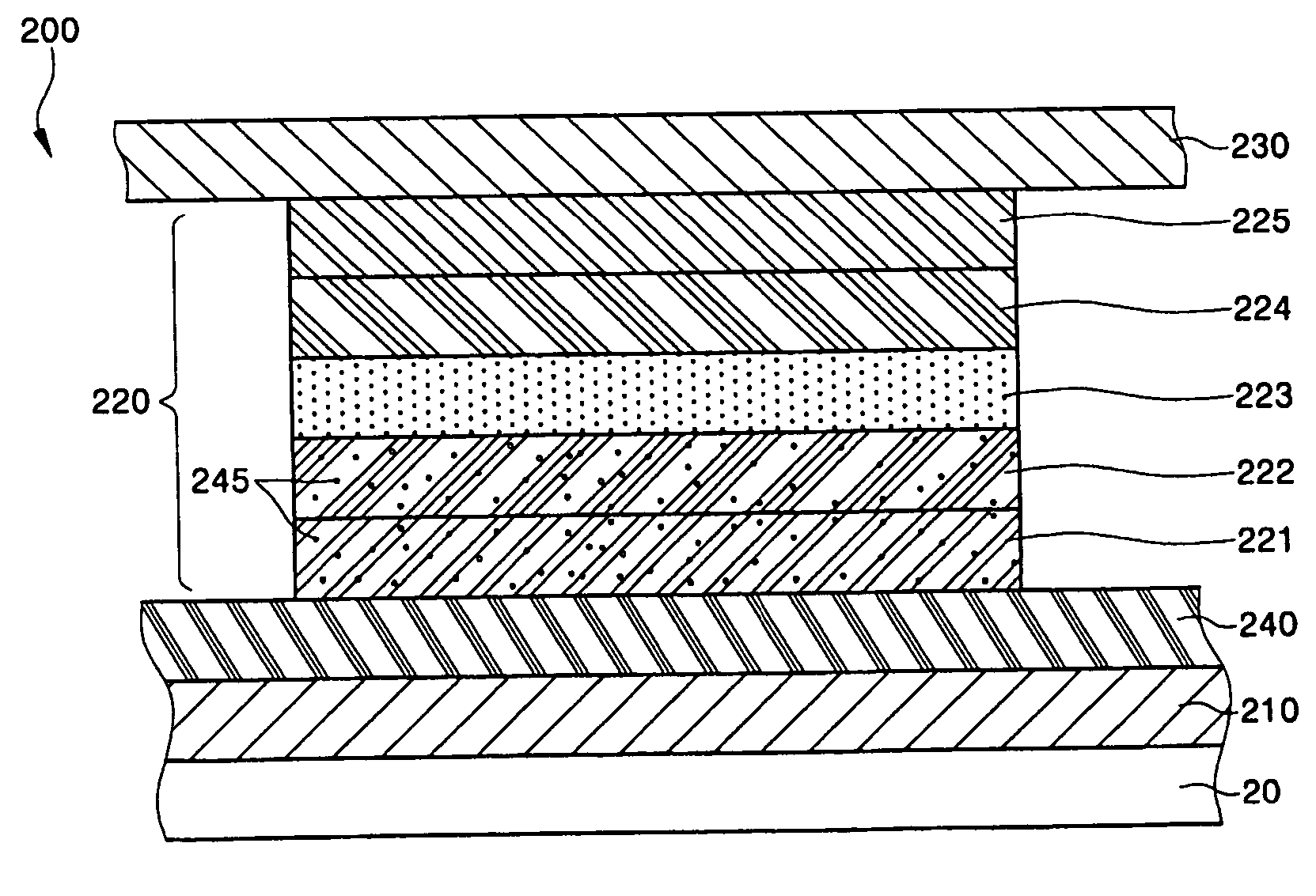
CROSS-REFERENCE TO RELATED APPLICATION [0001] This application claims priority to and the benefit of Korean Patent Application No. 10-2005-30500, filed Apr. 12, 2005 in the Korean Intellectual Property Office, the entire content of which is incorporated herein by reference. FIELD OF THE INVENTION [0002] The present invention relates to an organic light emitting device (OLED), and more particularly, to an OLED including a fullerene-based material or a layer doped with a fullerene-based material. BACKGROUND OF THE INVENTION [0003]FIG. 1 is a cross-sectional view of a conventional OLED. Referring to FIG. 1, a conventional OLED 100 generally includes an anode 110, an organic layer 120, and a cathode 130. The anode 110 is disposed on a substrate 10. The substrate 10 may have at least one thin film transistor (not shown) connected to the anode 110. The organic layer 120 is disposed on the anode 110 and includes an organic emission layer 123. The organic layer 120 may have several componen...
Claims
Login to View More Application Information
Patent Timeline
 IPC IPC(8): H05B33/00
CPCB82Y10/00H01L51/0046H01L51/5088H01L51/5048H01L51/5052H01L51/0081H10K85/211H10K85/324H10K50/155H10K50/14H10K50/17H05B33/12Y10S428/917H10K85/633H10K50/15
InventorLEE, JUN-YEOBCHUN, MIN-SEUNG
OwnerSAMSUNG DISPLAY CO LTD