Multichip package or system-in package

a multi-chip or system-in-one technology, applied in semiconductor devices, semiconductor/solid-state device details, instruments, etc., can solve the problems of limiting the wiring area that can be allocated to each power supply, unable to obtain sufficient areas, and no logic chips or memory chips employing a single power supply, etc., to achieve low noise and high operational reliability.

Inactive Publication Date: 2006-10-12
HITACHI LTD +1
View PDF6 Cites 30 Cited by
  • Summary
  • Abstract
  • Description
  • Claims
  • Application Information

AI Technical Summary

Benefits of technology

[0019] According to the present invention, it is possible to provide a multichip package or system-in package that features low noise and high operational reliability.

Problems solved by technology

Accordingly, if these signal lines are all routed (leaded) via test-only pins to the package exterior, sufficient areas cannot be obtained since the presence of the clearances of the signal wiring and the through-holes in the signal lines will form the power supply / GND (grounding) layers of the package substrate into an island shape.
However, there are no logic chips or memory chips employing a single power supply.
In the MCP / SiP, therefore, many kinds of power supply layers exist and this limits the wiring area that can be allocated to each power supply.
Also, the presence of the test-use wiring up to the test-only pins limits the power supply wiring areas to even smaller values, thus increasing the supply voltage noise level of the chip within the package.

Method used


Image

  • Multichip package or system-in package
  • Multichip package or system-in package
  • Multichip package or system-in package

Examples


first embodiment

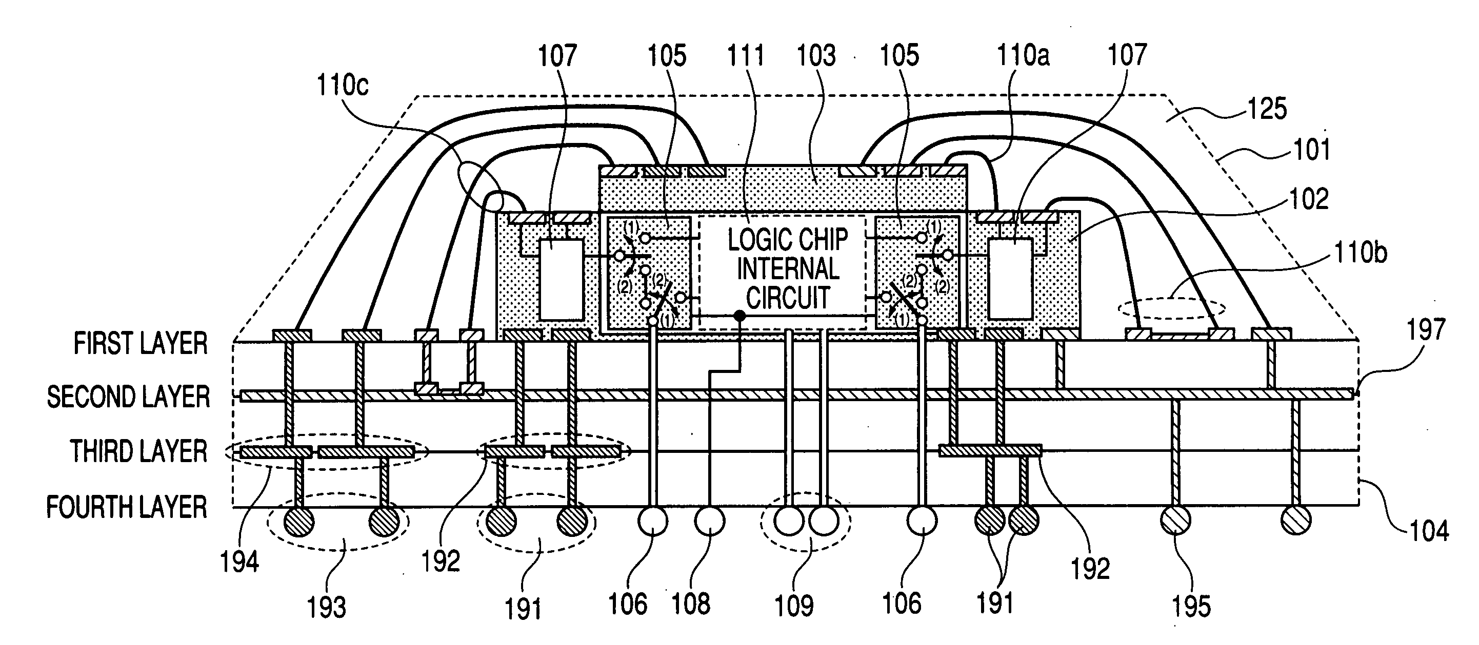
[0030]FIG. 1 is a front sectional view of a first embodiment, showing a mounting structure of a typical multichip package or system-in package according to the present invention.

[0031] The first embodiment of a multichip package (MCP) or system-in package (SiP) 101 in FIG. 1 includes one logic chip 102, one or more low-power-consumption memory chips 103 for a hand-held device, and a package substrate 104 for mounting the two types of chips. The MCP or SiP 101 is constructed by mounting the logic chip 102 and the memory chip(s) 103 in an electrically connected condition on the package substrate 104 and then sealing both of the two types of chips with a resin 125. The logic chip 102 and the low-power-consumption memory chip(s) 103 may be constructed in stacked or horizontally mounted form on the package substrate 104. For multiple memory chips 103, however, stacked construction is excellent in that there is no need to increase the package substrate 104 in area.

[0032] The following d...

second embodiment

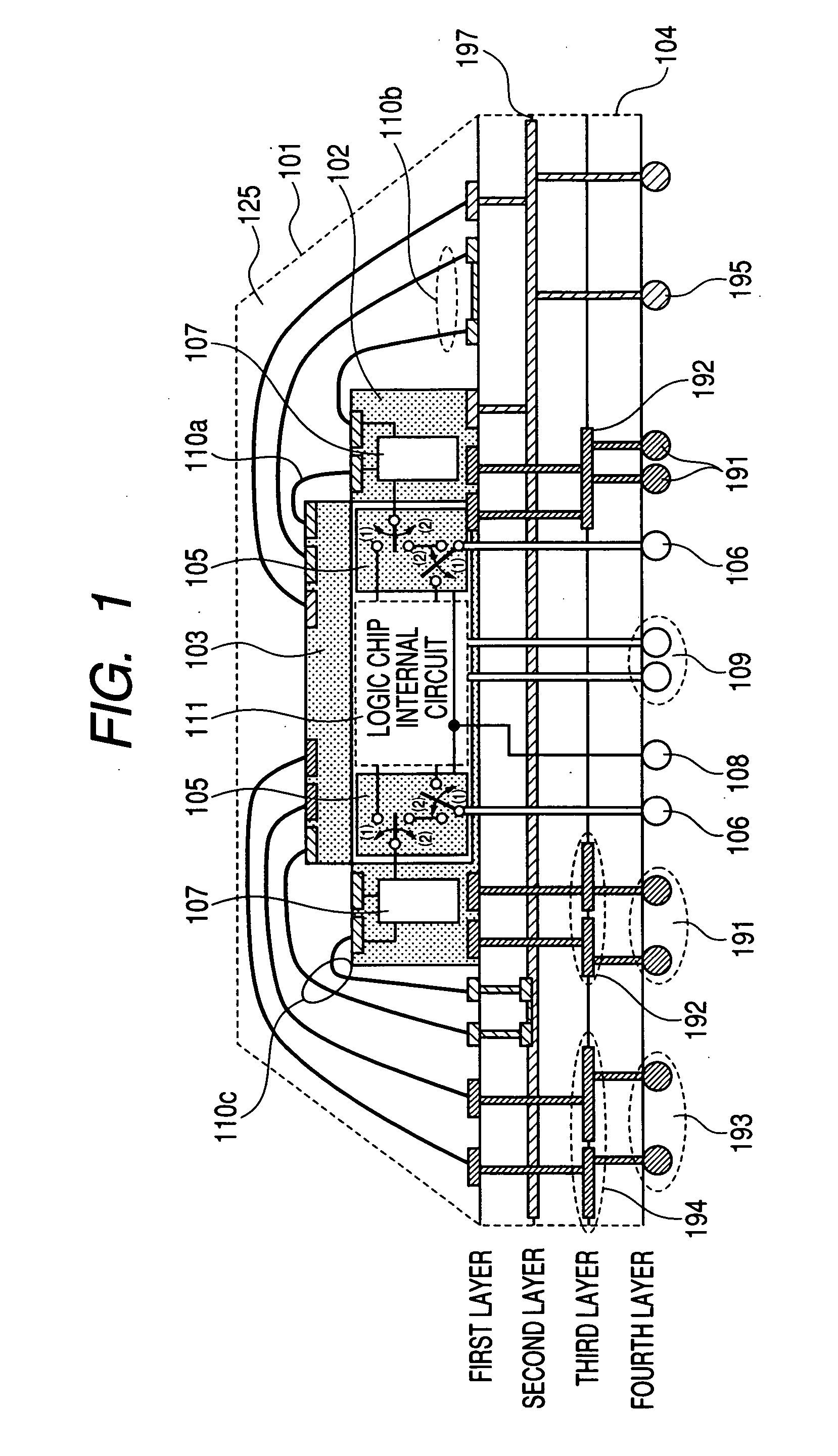
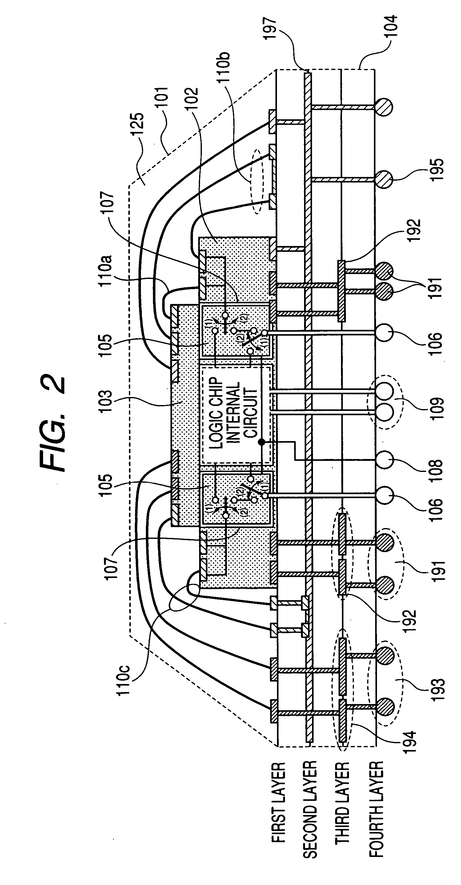
[0043]FIG. 4 is a front sectional view of a second embodiment, showing a mounting structure of another typical multichip package or system-in package according to the present invention. FIG. 5 is a block diagram showing the second embodiment of a multichip package or system-in package according to the present invention.

[0044] The second embodiment differs from the first embodiment in that a logic chip 102 includes, in a chip internal circuit, a test pattern generating circuit 201 which, for memory testing, generates a test pattern (i.e., an address signal, a data signal, and command signals such as / RAS and / CAS), thus enabling memory chip testing. Consequently, it is possible to make the test pattern generating circuit 201 valid within the logic chip 102 by giving a mode select signal (“High” or “Low” logical level signal or a rising / falling edge signal) from a mode select signal pin 108 or giving a test mode command signal from a logic signal pin 109. It is thus possible to test ...


PUM


Abstract

Disclosed is a multichip package or system-in package which the logic chip includes a selector circuit which, by transmitting a test mode select signal or a test mode select command to the logic chip, enables access from a logic signal pin connected to the logic chip, to a memory control signal to each of the “m” number of memory chips; and the memory control signal, when viewed from the logic chip, is connected using a one-for-one wiring scheme or a one-for-up-to-m branch wiring scheme, between the selector circuit and each of the “m” number of memory chips. This multichip package or system-in package is low in noise and high in operational reliability.

Description

BACKGROUND OF THE INVENTION [0001] 1. Field of the Invention [0002] The present invention relates to a multichip package or system-in package constructed by mounting, on a package substrate, not only one or more low-power-consumption memory chips for use in hand-held devices, but also a logic chip for controlling the memory chips. [0003] 2. Description of the Related Art [0004] Examples of the known multichip packages (MCPs) or system-in packages (SiPs) each constructed by mounting a plurality of low-power-consumption memory chips for a hand-held device, and a logic chip, in stacked or planar form in one package, are disclosed in Japanese Patent Laid-Open Nos. 2004-31754 and 2001-196526. These MCPs / SiPs require operational testing of memory provided therein after the packaging. In order to inherit existing testers and / or test patterns and enable direct access from the outside of the package to the memory, in the current MCPs or SiPs, the data / address / control signals and other signal...

Claims


Application Information

Patent Timeline
Patent Type & Authority Applications(United States)
IPC IPC(8): G11C5/06
CPCG11C5/04G11C5/063G11C29/1201G11C29/48G11C2029/0401H01L2224/48145H01L2224/48227H01L2924/15192H01L2924/15311H01L2225/06568H01L2224/32145G11C2029/3602H01L2924/181H01L2924/00012
Inventor NAKAMURA, SATOSHISUGA, TAKASHIKATAGIRI, MITSUAKIHIROSE, YUKITOSHI
Owner HITACHI LTD
Why Eureka
Try Eureka