Non-volatile memory device and method of preventing hot electron program disturb phenomenon

a non-volatile memory and program technology, applied in static storage, digital storage, instruments, etc., can solve problems such as channel boosting disturb phenomenon, hot electron program disturb, and reduced memory cell size to 100 nm, and achieve the effect of weakening the electric field

Active Publication Date: 2006-10-12
SK HYNIX INC
View PDF2 Cites 76 Cited by
  • Summary
  • Abstract
  • Description
  • Claims
  • Application Information

AI Technical Summary

Benefits of technology

[0031] Embodiments of the present invention prevent program disturbance by hot electrons resulting in a weaker electric field between memory cells connected to edge word lines and a select transistor.

Problems solved by technology

However, additional disturb phenomena, such as channel boosting disturb and hot electron program disturb, occur as the size of memory cells is reduced to 100 nm or less.
Therefore, the smaller the size of the memory cells, the more severe the channel boosting disturb phenomenon by hot electrons.
This causes the MLC to have more severe channel boosting disturbance by the aforementioned hot electrons.

Method used


Image

  • Non-volatile memory device and method of preventing hot electron program disturb phenomenon
  • Non-volatile memory device and method of preventing hot electron program disturb phenomenon
  • Non-volatile memory device and method of preventing hot electron program disturb phenomenon

Examples


Embodiment Construction

[0053] Embodiments of the present invention will be described with reference to the accompanying drawings. These embodiments are provided so that those ordinary skilled in the art can understand the present invention. It should be appreciated that the embodiments of the present invention may be modified in various manners without departing from the scope of the present invention.

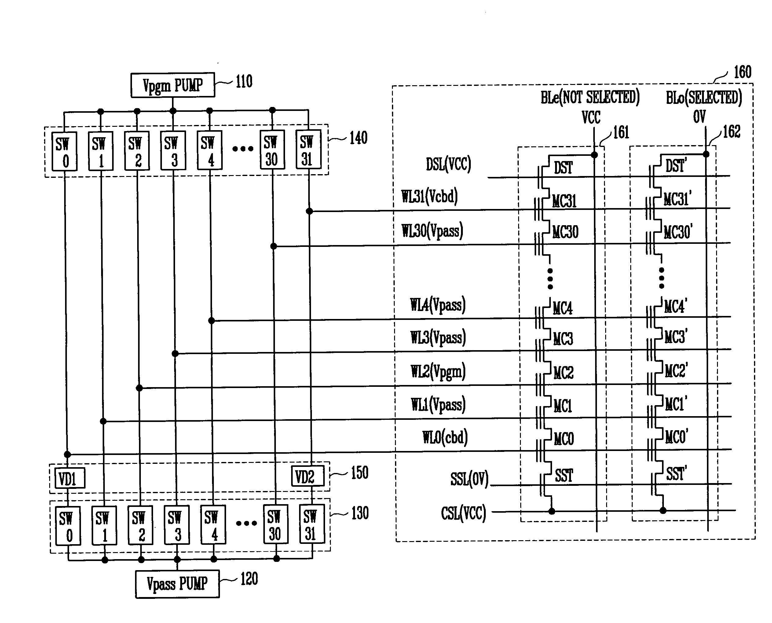
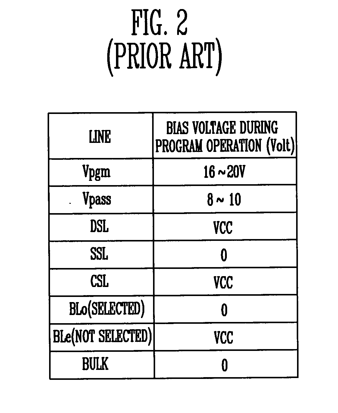
[0054]FIG. 6 is a circuit diagram of a NAND flash memory device according to one embodiment of the present invention. FIG. 7 is a table showing a program voltage condition of the NAND flash memory device shown in FIG. 6.

[0055] Referring to FIG. 6, the NAND flash memory device includes a Vpgm pump 110, a Vpass pump 120, switching units 130, 140, a voltage divider 150, and a memory cell array 160.

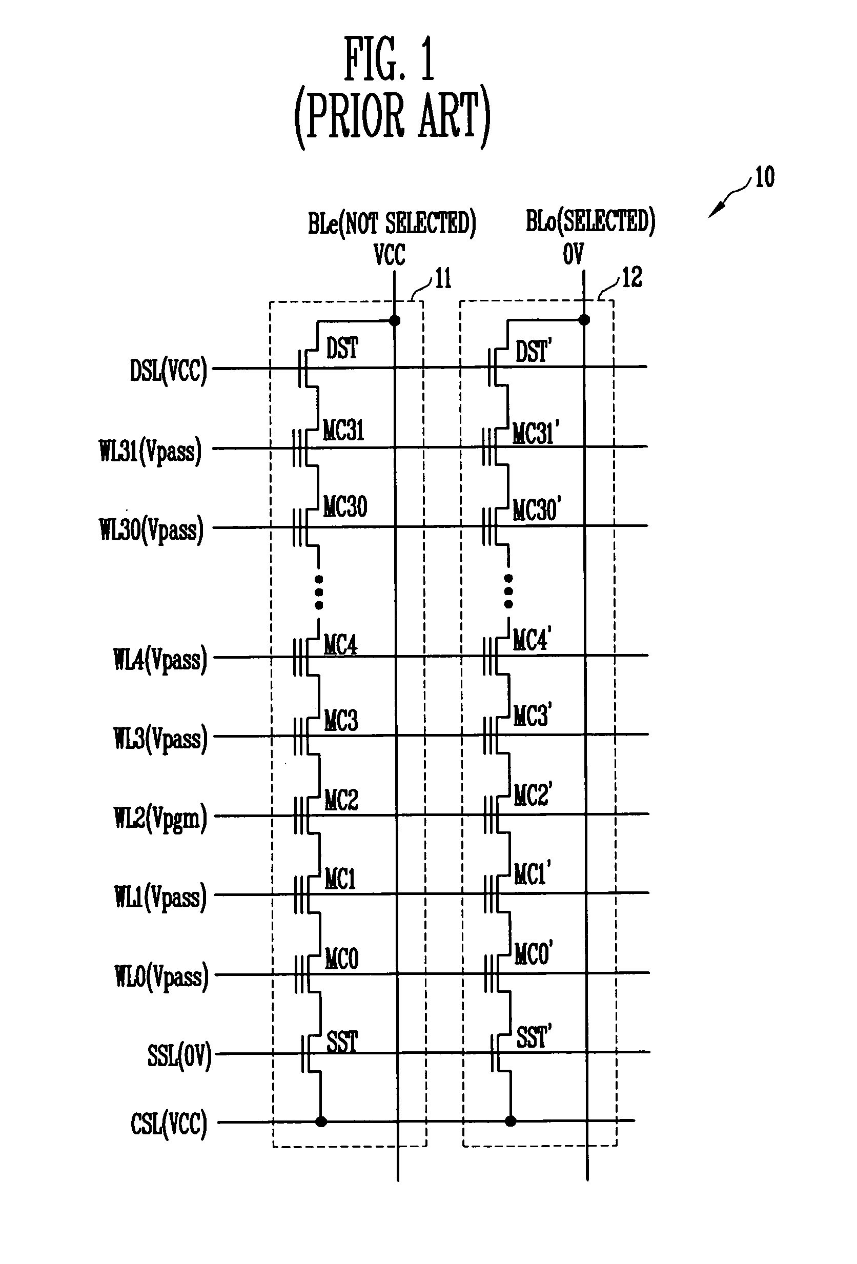
[0056] Memory cell array 160 includes memory cells MC, a source select transistor SST, and a drain select transistor DST. Bit lines BLe, BLo each acting as drains to memory cell array 160 are coupled to drain selec...


PUM


Abstract

A method for preventing generation of program disturbance incurred by hot electrons in a NAND flash memory device. A channel boosting disturb-prevention voltage lower than a program-prohibit voltage applied to other word lines is applied to edge word lines coupled to memory cells that are nearest to select transistors. As a result, an electric field between the memory cells coupled to the edge word lines and the select transistors is weakened, and the energy of the hot electrons is reduced.

Description

BACKGROUND [0001] 1. Field of the Invention [0002] The present invention relates to a non-volatile memory device and method of preventing a hot electron program disturb phenomenon, and more specifically, a method of preventing generation of program disturbance incurred by hot electrons in a NAND flash memory device. [0003] 2. Discussion of Related Art [0004] There is an increasing demand for semiconductor memory devices which can be electrically programmed and erased without a refresh function of rewriting data at a predetermined cycle. The term “program” refers to an operation of writing data into memory cells. [0005] In order to increase the level of integration of memory devices, a NAND flash memory device in which a plurality of memory cells is connected in series (i.e., a structure in which neighboring cells share the drain or source) to form one string has been developed. The NAND flash memory device is a memory device that sequentially reads information, unlike a NOR flash me...

Claims


Application Information

Patent Timeline
Patent Type & Authority Applications(United States)
IPC IPC(8): G11C16/04
CPCG11C16/3418G11C16/12G11C11/5621G11C16/0483
Inventor JOO, SEOK JIN
Owner SK HYNIX INC
Why Eureka
Try Eureka