Semiconductor structures and methods of forming them

A technology of semiconductor and gate structure, applied in the field of semiconductor structure and its formation, can solve problems such as serious gate-induced drain leakage current, and achieve the effect of reducing leakage current

Active Publication Date: 2022-04-15
SEMICON MFG INT (SHANGHAI) CORP +1
View PDF10 Cites 0 Cited by
  • Summary
  • Abstract
  • Description
  • Claims
  • Application Information

AI Technical Summary

Problems solved by technology

[0004] However, the gate-induced drain leakage current of semiconductor devices formed by prior art is still serious

Method used


Image

  • Semiconductor structures and methods of forming them
  • Semiconductor structures and methods of forming them
  • Semiconductor structures and methods of forming them

Examples


Embodiment Construction

[0032] As described in the background, the gate-induced drain leakage current of the semiconductor device is serious.

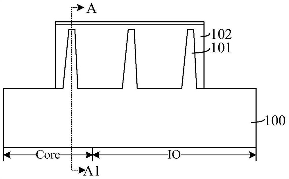
[0033] figure 1 with figure 2 A schematic diagram of a semiconductor structure.

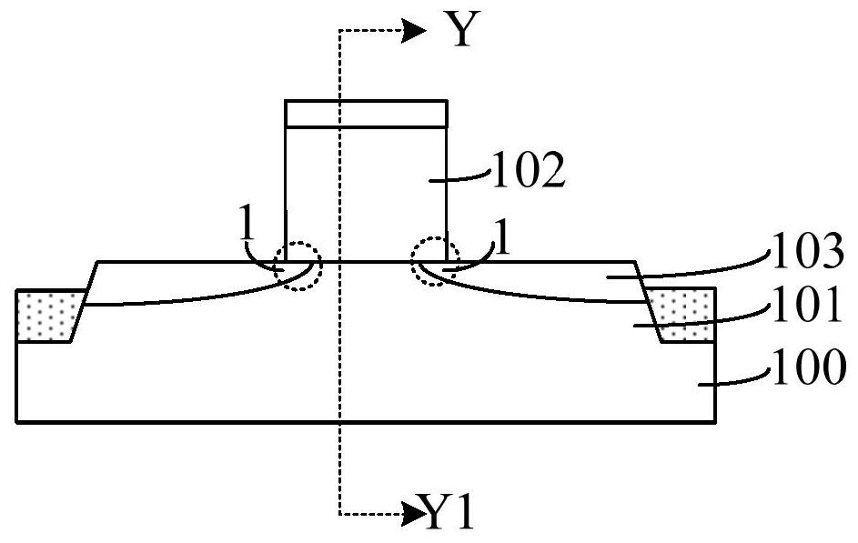
[0034] Please refer to figure 1 with figure 2 , figure 2 yes figure 1 A schematic sectional view along line AA1, figure 1 yes figure 2 A schematic cross-sectional view along the Y-Y1 line, a substrate 100, the substrate 100 includes a Core region and an IO region, the Core region and the IO region respectively have several fins 101 on the substrate 100; a gate structure 102 across the fins 101 ; The source and drain doped regions 103 in the fin portion 101 located on both sides of the gate structure 102 .

[0035]In the above method, since the step of forming the source-drain doped region 103 includes: forming a source-drain opening in the fin portion 101 on both sides of the gate structure 102; forming an epitaxial layer in the source-drain opening; Doping ions int...


PUM

PropertyMeasurementUnit
thicknessaaaaaaaaaa
thicknessaaaaaaaaaa
thicknessaaaaaaaaaa

Abstract

A semiconductor structure and a method for forming the same, wherein the method includes: providing a base with fins on the base; performing amorphization treatment on the top of the fins, forming an amorphous region on the top of the fins; A capping layer is formed on the top surface of the amorphous region; a recrystallization treatment is performed so that the amorphous region and the capping layer form a recrystallization layer; a gate structure and source-drain doped regions respectively located on both sides of the gate structure are formed, The gate structure spans the recrystallized layer and the fin, and the gate structure covers part of the surface of the recrystallized layer and part of the sidewall surface of the fin, and the source-drain doped region is located in the recrystallized layer . The method can reduce the gate induced drain leakage current of the device.

Description

technical field [0001] The invention relates to the field of semiconductor manufacturing, in particular to a semiconductor structure and a forming method thereof. Background technique [0002] Because there is a large overlapping area between the gate and the drain of a metal oxide semiconductor field effect transistor (Metal Oxide Semiconductor Field Effect Transistor, MOSFET). Taking NMOSFET as an example, when a voltage is applied to the gate, the drain potential in the NMOSFET is more positive than the gate potential, and holes will be generated in the overlapping region due to the effect of the gate voltage, and the holes will pass through The over-depletion region moves into the substrate and forms a substrate current, which is usually a gate-induced drain leakage (Gate-Induced Drain Leakage, GIDL) current. Conversely, when a voltage is applied to the gate, the gate potential in the PMOSFET is more positive than the drain potential, and electrons are generated in the ...

Claims


Application Information

Patent Timeline
Patent Type & Authority Patents(China)
IPC IPC(8): H01L21/336H01L21/28H01L29/06H01L29/423H01L29/78
CPCH01L29/0638H01L29/4236H01L29/66795H01L29/785
Inventor 李勇
Owner SEMICON MFG INT (SHANGHAI) CORP
Why Eureka
Try Eureka