Silicon carbide JBS device and manufacturing method thereof

A manufacturing method and technology of silicon carbide, applied in semiconductor/solid-state device manufacturing, semiconductor devices, electrical components, etc., can solve the problems of sacrificing reverse performance, complicated process, and high cost

Pending Publication Date: 2022-02-01
重庆平创半导体研究院有限责任公司
View PDF0 Cites 0 Cited by
  • Summary
  • Abstract
  • Description
  • Claims
  • Application Information

AI Technical Summary

Problems solved by technology

This technology introduces a low barrier Schottky metal between the two P-type regions to improve the forward conduction voltage drop. At the same time, this technology also causes an increase in the reverse leakage current of the device, sacrificing the reverse performance
In addition, due to the introduction of two Schottky barrier metals, the process is complicated and the cost is high

Method used


Image

  • Silicon carbide JBS device and manufacturing method thereof
  • Silicon carbide JBS device and manufacturing method thereof
  • Silicon carbide JBS device and manufacturing method thereof

Examples


Embodiment 1

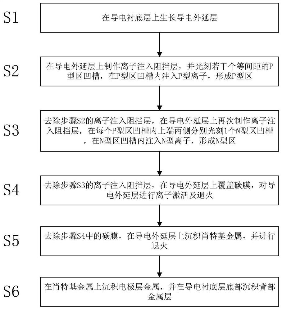
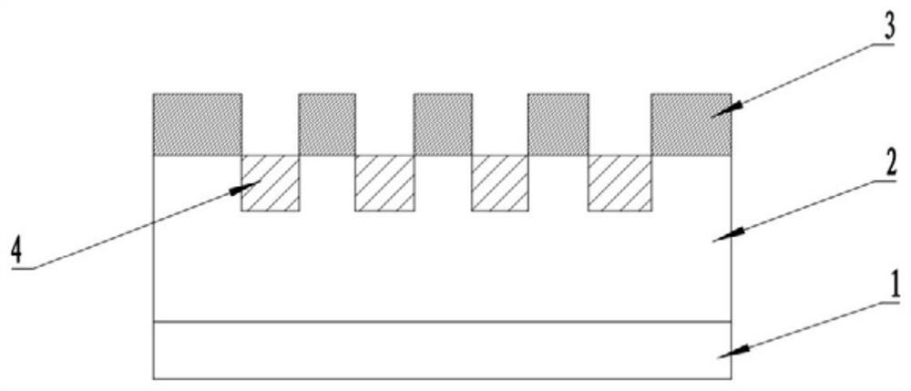
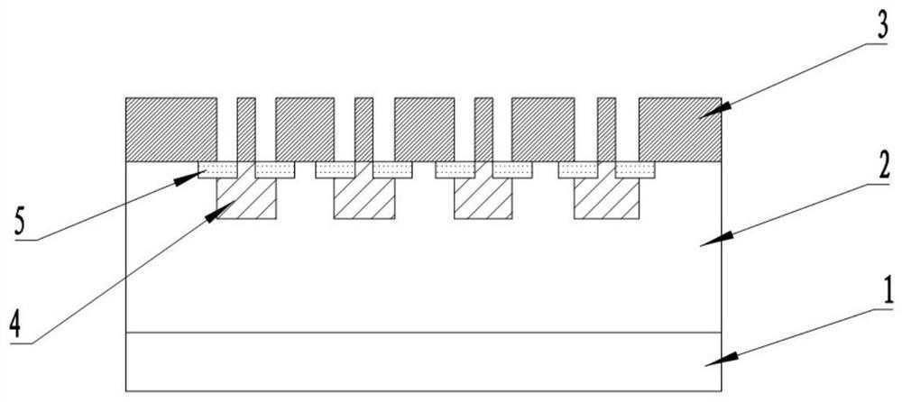
[0040] Such as Figure 5 As shown, a silicon carbide JBS device is disclosed in this embodiment, the device includes a conductive substrate layer 1 and a conductive epitaxial layer 2, the ion doping concentration of the conductive epitaxial layer 2 is 1e16cm-3, and the thickness of the conductive epitaxial layer 2 is 3 μm.

[0041] The conductive epitaxial layer 2 is provided with a P-type region 4 and an N-type region 5, and the P-type region 4 includes a plurality of equally spaced P-type region 4 grooves, and P-type ions are implanted in the P-type region 4 grooves. ; Both sides of the upper end of each P-type area 4 grooves are respectively provided with an N-type area 5 grooves, and N-type ions are injected into the N-type area 5 grooves, the P-type ions are aluminum ions, and the aluminum The ion implantation dose is 1e11cm-3, the N-type ions are nitrogen ions, and the nitrogen ion implantation dose is 5e11cm-3.

[0042] Schottky metal 6 is deposited on the upper part ...

Embodiment 2

[0051] This embodiment also discloses a silicon carbide JBS device, which differs from the first embodiment in that the ion doping concentration of the conductive epitaxial layer 2 in this embodiment is 1e18cm-3, and the thickness of the conductive epitaxial layer 2 is 52 μm. The P-type ions are aluminum ions, and the implantation dose of the aluminum ions is 1e13cm-3. The N-type ions are nitrogen ions, and the nitrogen ion implantation dose is 5e14cm-3. The electrode layer metal 7 is made of aluminum with a thickness of 5 μm, and the back metal layer 8 is made of nickel with a thickness of 3 μm.

[0052] This embodiment also discloses a silicon carbide JBS manufacturing method that is matched with the above-mentioned silicon carbide JBS device. The difference from Embodiment 1 is that in this embodiment,

[0053] S1: The ion doping concentration of the conductive epitaxial layer 2 is 1e18cm-3, and the thickness of the conductive epitaxial layer 2 is 52 μm.

[0054] S2: the ...

Embodiment 3

[0060] Such as Image 6 As shown, this embodiment also discloses a silicon carbide JBS device. The difference from Embodiment 1 is that this embodiment also includes a buffer layer, and the buffer layer is respectively connected to the conductive substrate layer 1 and the conductive epitaxial layer 2. , the buffer layer is N-type doped silicon carbide. The ion doping concentration of the conductive epitaxial layer 2 is 1e19cm-3, and the thickness of the conductive epitaxial layer 2 is 100 μm. The P-type ions are aluminum ions, and the implantation dose of the aluminum ions is 1e14cm-3. The N-type ions are nitrogen ions, and the nitrogen ion implantation dose is 1e15cm-3. The material of the electrode layer metal 7 is aluminum with a thickness of 7 μm, and the material of the back metal layer 8 is silver with a thickness of 4 μm.

[0061] This embodiment also discloses a silicon carbide JBS manufacturing method that is matched with the above-mentioned silicon carbide JBS dev...


PUM

PropertyMeasurementUnit
thicknessaaaaaaaaaa
thicknessaaaaaaaaaa
thicknessaaaaaaaaaa

Abstract

The invention relates to the technical field of semiconductors, and discloses a silicon carbide JBS device and a manufacturing method thereof. The manufacturing method comprises the steps of S1, growing a conductive epitaxial layer on a conductive substrate layer; S2, photoetching a P-type region groove on the conductive epitaxial layer, and injecting P-type ions into the P-type region groove to form a P-type region; S3, photoetching an N-type region groove on each of the two sides of the upper end in each P-type region groove, and injecting N-type ions into the N-type region grooves to form an N-type region; S4, performing ion activation and annealing on the conductive epitaxial layer; S5, depositing Schottky metal on the conductive epitaxial layer; and S6, depositing electrode layer metal on the Schottky metal, and depositing a back metal layer at the bottom of the conductive substrate layer. According to the silicon carbide JBS device and the manufacturing method thereof, the forward characteristic of a diode can be improved, the forward conduction voltage of the diode device is reduced, the current density is improved, meanwhile, the reverse leakage current performance of the device is not reduced, the process is simple, and the cost is low.

Description

technical field [0001] The invention relates to the technical field of semiconductors, in particular to a silicon carbide JBS device and a manufacturing method thereof. Background technique [0002] As a typical representative of the third-generation semiconductor material, silicon carbide has a larger band gap and higher thermal conductivity than traditional silicon materials. Corresponding silicon carbide devices have higher operating frequencies and higher thermal conductivity than silicon devices. Small loss and higher operating temperature and power density are widely used in new energy vehicles, high-power power supplies and other fields. Silicon carbide junction Schottky diode devices have the characteristics of low conduction voltage drop, high reverse recovery speed and low leakage current of Schottky diodes, and have been extensively studied by people. Due to the high turn-on voltage drop of the SiC PN junction, which is about 2.7V, it is difficult for the traditi...

Claims


Application Information

Patent Timeline
Patent Type & Authority Applications(China)
IPC IPC(8): H01L21/04H01L29/872H01L29/06H01L29/47
CPCH01L21/0445H01L21/046H01L21/0495H01L29/6606H01L29/872H01L29/0619H01L29/47
Inventor 陈显平罗厚彩钱靖
Owner 重庆平创半导体研究院有限责任公司
Why Eureka
Try Eureka