LDMOS device and forming method thereof

A technology of device and extension direction, which is applied in the field of LDMOS devices and its formation, can solve the problems that the electrical performance of lateral double-diffused field effect transistors needs to be improved, and achieve the effect of optimizing electrical performance

Active Publication Date: 2019-12-31
SEMICON MFG INT (SHANGHAI) CORP +1
View PDF4 Cites 1 Cited by
  • Summary
  • Abstract
  • Description
  • Claims
  • Application Information

AI Technical Summary

Problems solved by technology

[0004]The electrical performance of the existing lateral double diffused field effect transistor (LDMOS) needs to be improved

Method used


Image

  • LDMOS device and forming method thereof
  • LDMOS device and forming method thereof
  • LDMOS device and forming method thereof

Examples


Embodiment Construction

[0039] It can be seen from the background art that the electrical performance of the LDMOS device still needs to be improved. The reason is analyzed in conjunction with the structure of an LDMOS device.

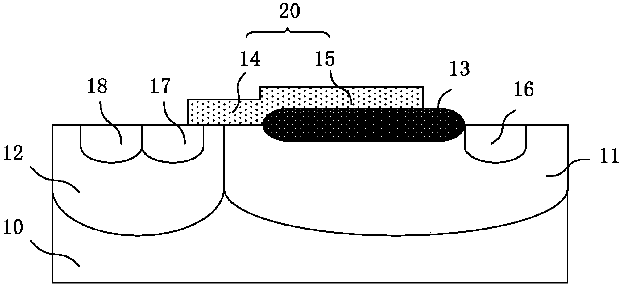
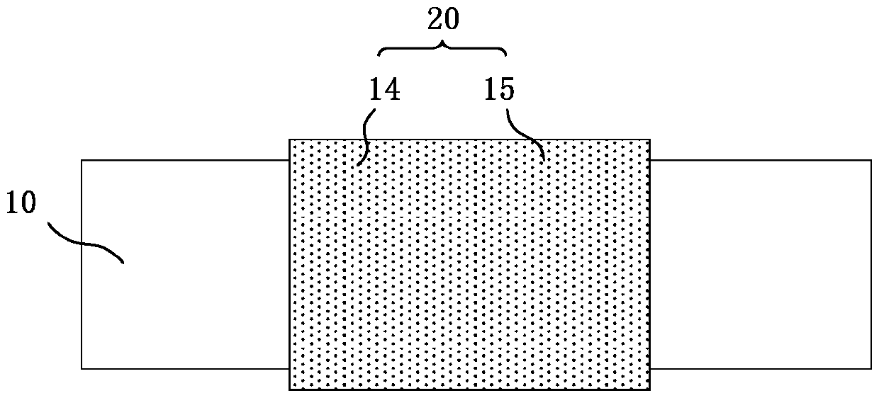
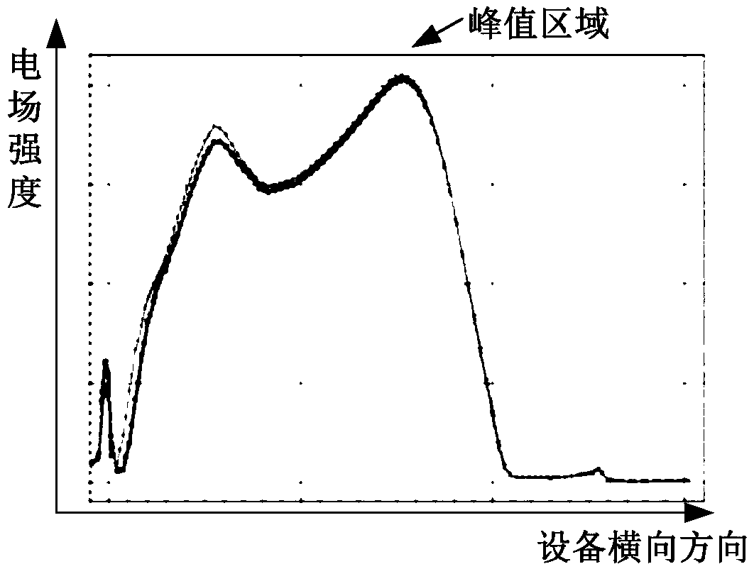
[0040] refer to Figure 1 to Figure 3 , figure 1 A schematic structural diagram of an LDMOS device is shown, figure 2 yes figure 1 The top view of the LDMOS device shown, image 3 yes figure 1 The electric field strength change curve of the LDMOS device shown.

[0041] combined reference figure 1 and figure 2 , figure 2 Only the substrate and the gate structure are illustrated, and an LDMOS device is provided, which includes: a substrate 10, the substrate 10 includes a drift region 11 and a well region 12 adjacent to the drift region 11; a field oxide layer 13 , located on the substrate 10 of the drift region 11; a gate structure 20, comprising a gate electrode 14 and a field plate 15 covering part of the field oxide layer 13 and the substrate 10, the gate electro...


PUM


Abstract

The invention relates to an LDMOS device and a forming method thereof. The LDMOS device comprises a substrate, a field oxide layer, a gate structure, a drain region and a source region, wherein the substrate comprises a drift region; the field oxide layer is positioned on the substrate of the drift region; the gate structure comprises a gate electrode covering part of the field oxide layer and thesubstrate and a field plate adjacent to the gate electrode, the extending direction of the gate electrode is a first direction, the direction, perpendicular to the first direction, on the projectionplane of the substrate is a second direction, the field plate comprises a plurality of pseudo gate structures in the first direction and the second direction, and the pseudo gate structures are located on the field oxide layer; the drain region is positioned in the drift region on one side of the field plate; and the source region is positioned in the substrate on one side of the gate electrode. The field plate of the LDMOS device comprises the plurality of pseudo gate structures, and the gaps are reserved between the pseudo gate structures, so that the electric field intensity between the field plate close to one side of the drain end and the drift region can be reduced, and the electrical performance of the LDMOS device is optimized.

Description

technical field [0001] The invention relates to the field of semiconductors, in particular to an LDMOS device and a forming method thereof. Background technique [0002] Lateral Double-Diffused MOSFET (LDMOS, Lateral Double-Diffused MOSFET) is mainly used in power integrated circuits, such as RF power amplifiers for mobile phone base stations, and can also be used in high frequency (HF), very high frequency (VHF) and ultra-high frequency (UHF) High frequency (UHF) broadcast transmitters and microwave radar and navigation systems, etc. LDMOS technology brings higher power peak-to-average ratio, higher gain and linearity to the new generation of base station amplifiers, and at the same time brings higher data transmission rates to multimedia services. [0003] In the lateral double-diffused field effect transistor (LDMOS), obtaining a uniform electric field at the bottom of the field oxide layer in the drift region is the key to this type of device. The electric field is affe...

Claims


Application Information

Patent Timeline
Patent Type & Authority Applications(China)
IPC IPC(8): H01L29/78H01L29/06H01L29/423H01L29/40H01L21/336
CPCH01L29/7816H01L29/0684H01L29/42356H01L29/402H01L29/66477
Inventor 杨震马燕春郭兵王孝远王刚宁
Owner SEMICON MFG INT (SHANGHAI) CORP
Why Eureka
Try Eureka