Nonvolatile semiconductor memory including redundant cell for replacing defective cell

a technology of semiconductor memory and redundant cells, which is applied in the field of nonvolatile semiconductor memory, can solve the problems of huge test cost, inability to replace defective cells with redundant cells, and inability to meet the requirements of testing,

Active Publication Date: 2006-10-12
KIOXIA CORP
View PDF6 Cites 8 Cited by
  • Summary
  • Abstract
  • Description
  • Claims
  • Application Information

AI Technical Summary

Problems solved by technology

Also, defects caused by data rewrite on the market exist on the order of a few ten to a few hundred ppm.
Therefore, to decrease the percent defective by finding a defective cell by screening and replacing it with a redundant cell, a very long test time is necessary, and this produces an enormous test cost.
Accordingly, it is practically difficult to replace a defective cell with a redundant cell by screening.
As a consequence, a nonvolatile semiconductor memory (chip) is often regarded as a defective product although usable redundant cells exist in the device.

Method used


Image

  • Nonvolatile semiconductor memory including redundant cell for replacing defective cell
  • Nonvolatile semiconductor memory including redundant cell for replacing defective cell
  • Nonvolatile semiconductor memory including redundant cell for replacing defective cell

Examples


first embodiment

[0020] First, a nonvolatile semiconductor memory of the first embodiment of the present invention will be explained below.

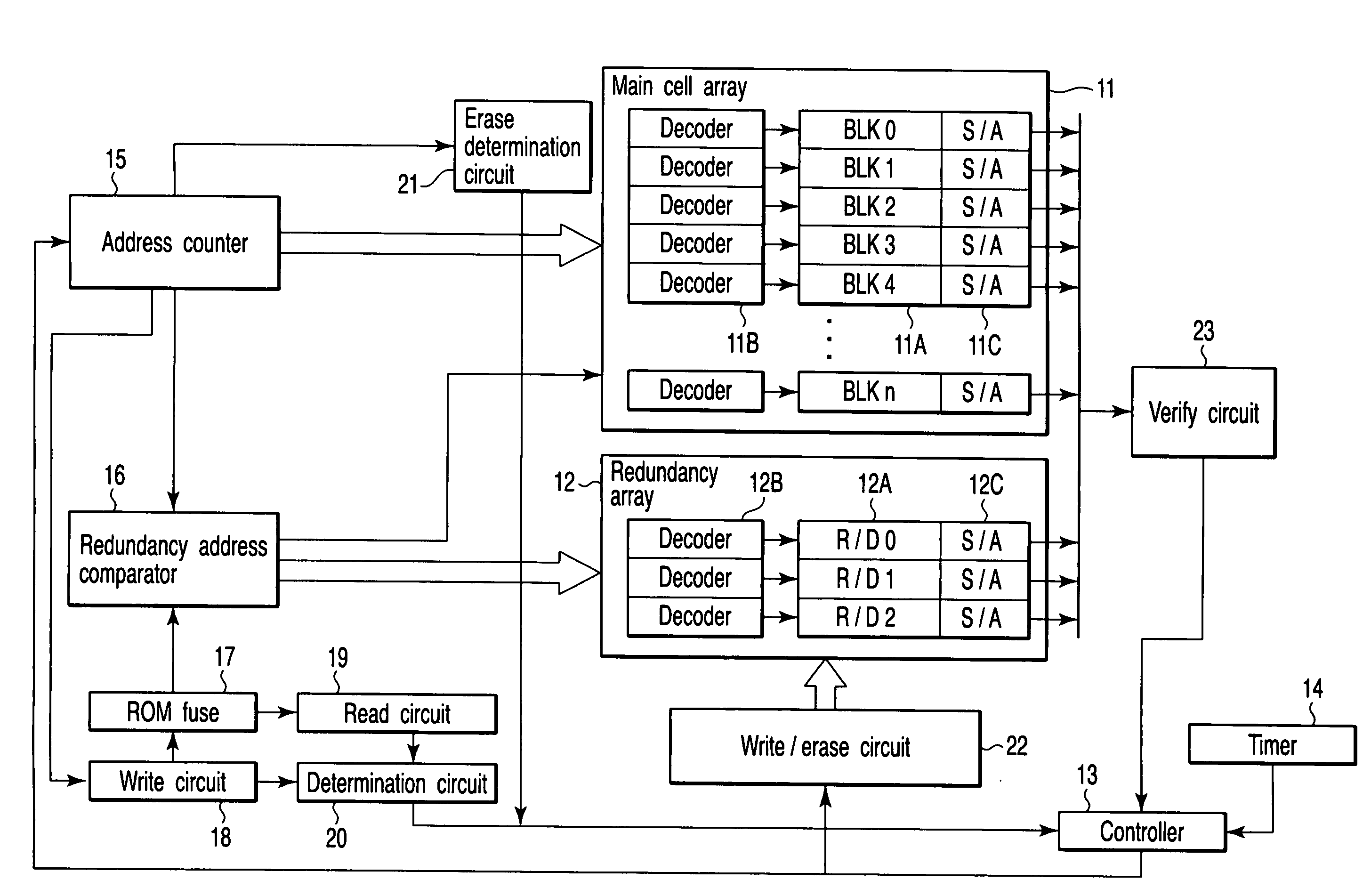
[0021]FIG. 1 is a block diagram showing the arrangement of the nonvolatile semiconductor memory of the first embodiment.

[0022] As shown in FIG. 1, this nonvolatile semiconductor memory comprises a memory cell array including a main cell array 11 and redundancy array 12, a controller 13, a timer 14, an address counter 15, a redundancy address comparator 16, a ROM fuse 17, a write circuit 18, a read circuit 19, a determination circuit 20, an erase determination circuit 21, a write / erase circuit 22, and a verify circuit 23.

[0023] In the main cell array 11, a plurality of blocks (BLK0, BLK1, . . . , BLKn) 11A are arranged. A decoder 11B and sense amplifier 11C are connected to each of the blocks (BLK0, BLK1, . . . , BLKn) 11A. Each of the blocks (BLK0, BLK1, . . . , BLKn) 11A includes a plurality of memory cells, and these memory cells in the block are erased at o...

second embodiment

[0055] A nonvolatile semiconductor memory of the second embodiment of the present invention will be described below. The same reference numerals as in the first embodiment denote the same parts to omit an explanation thereof, and only different parts will be explained below. The first embodiment uses the method of searching a plurality of redundant blocks for an unused redundant block. In the second embodiment, a specific redundant block is formed as a block to be exclusively used in an “automatic redundant block replacement routine”.

[0056]FIG. 5 is a block diagram showing the arrangement of the nonvolatile semiconductor memory of the second embodiment.

[0057] In a redundancy array 12, a plurality of redundant blocks (R / D0 and R / D1) 12A and an automatic redundant block (Auto R / D) 12AA are arranged. A decoder 12B and sense amplifier 12C are connected to each of the redundant blocks (R / D0 and R / D1) 12A and automatic redundant block 12AA. Each of the redundant blocks (R / D0 and R / D1) 1...

third embodiment

[0068] A nonvolatile semiconductor memory of the third embodiment of the present invention will be explained below.

[0069] In the first and second embodiments, the automatic redundant block replacement routine starts when two seconds elapse from the start of block erase, and this set time is very long. Accordingly, it takes a very long time to check the operation in the test step. In the third embodiment, therefore, as shown in FIG. 7, in order to reduce the time required to check the operation in the test step, the transition time from the start of block erase to the automatic redundant block replacement routine is set to a few ten μs, e.g., 10 μs (step S41). The rest of the arrangement is the same as in the first and second embodiments.

[0070] The embodiments of the present invention relate to replacement of a redundant cell in a nonvolatile semiconductor memory. If an erase operation currently being executed is not completed within a predetermined time, a block to be erased can b...


PUM


Abstract

A nonvolatile semiconductor memory includes a cell array, redundancy array, erase circuit, timer, and controller. The cell array has a plurality of memory cells. The redundancy array has a plurality of redundant cells capable of replacing the memory cell. The erase circuit performs an erase operation on a target cell including the memory cell or the redundant cell. The timer measures the time elapsed from the start of the erase operation performed for the target cell by the erase circuit. The controller stops the erase operation and replaces the target cell with the redundant cell, when detecting that a predetermined time has elapsed from the start of the erase operation by the measurement of the elapsed time by the timer.

Description

CROSS-REFERENCE TO RELATED APPLICATIONS [0001] This application is based upon and claims the benefit of priority from prior Japanese Patent Application No. 2005-114749, filed Apr. 12, 2005, the entire contents of which are incorporated herein by reference. BACKGROUND OF THE INVENTION [0002] 1. Field of the Invention [0003] The present invention relates to a nonvolatile semiconductor memory and, more particularly, to a nonvolatile semiconductor memory including a redundant cell for replacing a defective cell or the like. [0004] 2. Description of the Related Art [0005] A nonvolatile semiconductor memory generally includes a redundant cell for replacing a defective cell in order to increase the yield as the memory capacity increases. [0006] Three general types of the redundant cell are: column redundancy for relieving a defect on each bit line; row redundancy for relieving a defect on each word line; and block redundancy for relieving a defect in each block. [0007] The types and number...

Claims


Application Information

Patent Timeline
Patent Type & Authority Applications(United States)
IPC IPC(8): G11C16/04
CPCG11C16/04G11C29/838G11C29/76G11C29/52F24D10/006F24D19/1015F24D2220/04F24D2220/042F24D2220/06Y02B30/00Y02E20/14
Inventor KASAI, TAKAMICHIKATO, HIDEO
Owner KIOXIA CORP
Why Eureka
Try Eureka