Versatile system for selective organic structure production

a selective organic structure and modular technology, applied in the direction of microstructure devices, solid-state devices, microstructure devices, etc., can solve the problems of devices being subjected to one or more intervening and possibly deleterious conditions, and achieve the effect of convenient implementation, high versatility and precise placemen

Inactive Publication Date: 2006-10-12
TEXAS INSTR INC
View PDF16 Cites 3 Cited by
  • Summary
  • Abstract
  • Description
  • Claims
  • Application Information

AI Technical Summary

Benefits of technology

[0007] The present invention provides a system for selective formation of organic structures within a semiconductor platform. The system of the present invention utilizes materials readily available within commercial semiconductor manufacturing processes, and enables efficient introduction of novel materials to such processes. The system of the present invention provides highly versatile and precise placement of one or more organic-type materials, throughout simple or complex structures. The system of the present invention is readily implemented without significantly increasing production overhead or cost. The system of the present invention thus addresses and overcomes a number of limitations associated with conventional approaches.
[0008] Specifically, the present invention provides a system that spatially directs or encodes one or more desired organic or biological materials to specific locations within or along a semiconductor structure. The present invention provides a system in which encoder materials or compounds are initially formed or placed where desired organic-type materials are needed or desired. The encoder materials are sufficiently robust to withstand necessary manufacturing processes and conditions—particularly deleterious ones (e.g., high temperature, plasma exposure). The eventual location of the desired organic-type materials may thus be encoded seamlessly at various points throughout a fabrication process, without requiring special construction processes.

Problems solved by technology

Once the encoder material has been disposed, the device may then be subjected to one or more intervening and possibly deleterious conditions, such as undercutting, throughout the remainder of device fabrication.

Method used


Image

  • Versatile system for selective organic structure production
  • Versatile system for selective organic structure production

Examples


Embodiment Construction

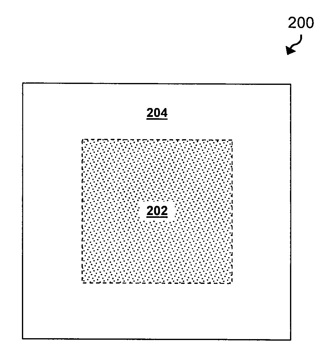
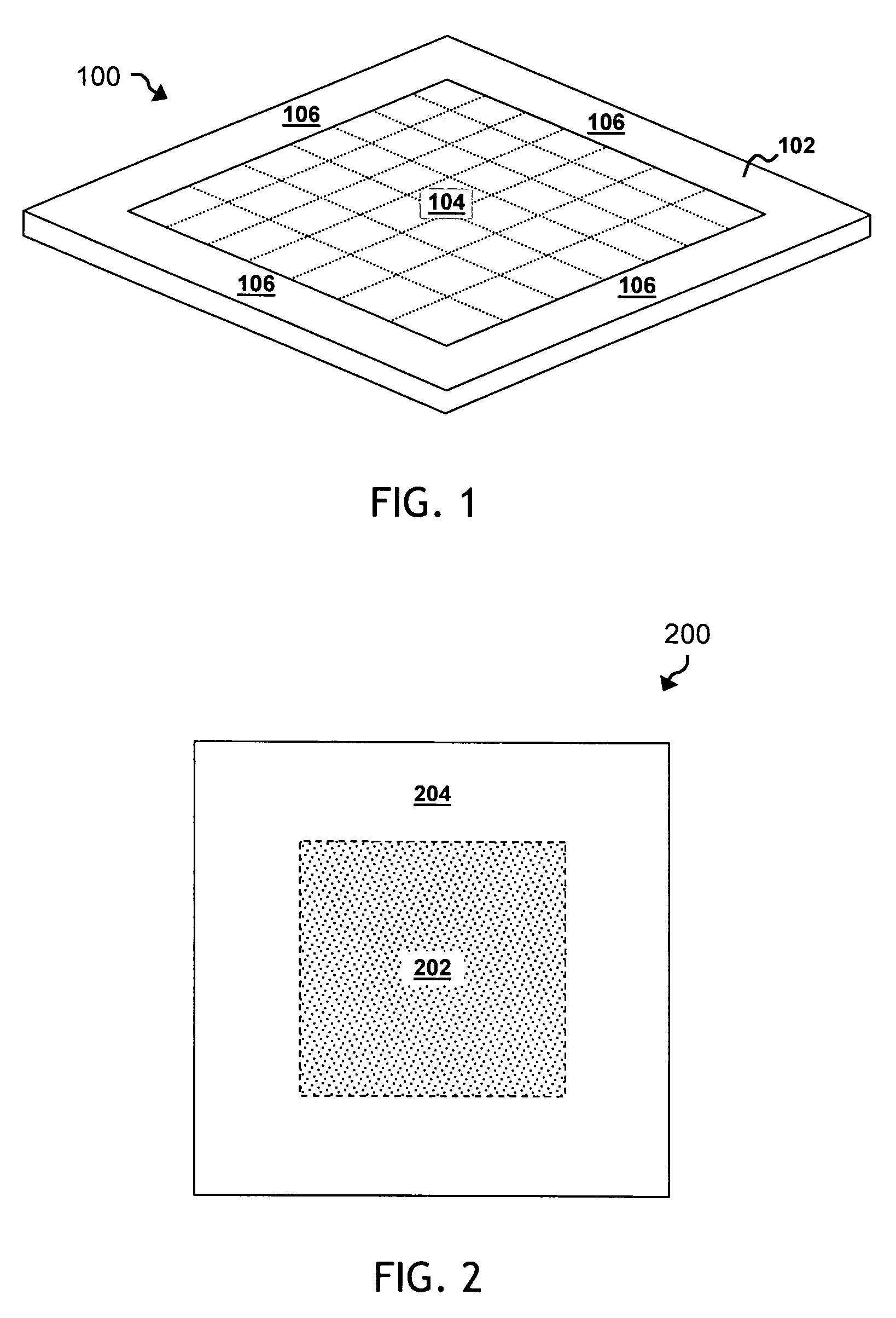
[0019] While the making and using of various embodiments of the present invention are discussed in detail below, it should be appreciated that the present invention provides many applicable inventive concepts, which can be embodied in a wide variety of specific contexts. For example, certain aspects of the present invention are described, for purposes of explanation and illustration, in conjunction with the placement of certain organic materials within a micro-electromechanical system (MEMS) device, using semiconductor manufacturing processes. Upon reference to the description of the present invention, however, it should be readily apparent that the principles and teachings of the present invention may be readily implemented with other device types, materials, or manufacturing systems where selective, precise, substitutional placement of an organic or biological material is required or desired. Therefore, the specific embodiments discussed herein are merely illustrative of specific ...


PUM


Abstract

The present invention provides a system for selectively forming an organic structure in a microelectromechanical device (100). According to the present invention, an encoder material is disposed along a surface (102) or substrate, to define a desired organic microstructure (104, 106). The encoder material may then be subjected to one or more intervening and possibly deleterious conditions, such as undercutting. Once such conditions are concluded, the encoder material is subjected to a stimulus that causes it to form the desired organic microstructure.

Description

TECHNICAL FIELD OF THE INVENTION [0001] The present invention relates generally to the field of semiconductor device manufacturing and, more particularly, to apparatus and methods for selective placement or formation of structures comprising organic materials or compounds. BACKGROUND OF THE INVENTION [0002] Semiconductor devices are ubiquitous in modern society, and this can largely be attributed to the success of wafer-scale semiconductor manufacturing processes. Semiconductor manufacturing infrastructure provides numerous prospects for the introduction and integration of new technologies within existing processes. Among recent developments, micro-electromechanical system (MEMS)—devices that have electrically controllable mechanical elements (such as actuators, gears, optical modulating elements, etc.)—have been formed monolithically on a semiconductor substrate using integrated circuit techniques. Further advances in the production of submicron scale electronic devices or systems ...

Claims


Application Information

Patent Timeline
Patent Type & Authority Applications(United States)
IPC IPC(8): H01L51/40
CPCB81C1/00206B82Y30/00B81C1/00492
Inventor MILLER, SETH ADRIAN
Owner TEXAS INSTR INC
Why Eureka
Try Eureka