Liquid crystal display

a technology of liquid crystal display and display panel, which is applied in the direction of electrical equipment, semiconductor devices, instruments, etc., can solve the problems of deteriorating aperture ratio, poor lateral visibility of va mode lcd, and inability to directly and correctly control the transmittance of the two sub-pixels to the desired level, etc., to achieve the effect of enhancing the lateral side visibility

Inactive Publication Date: 2006-10-19
SAMSUNG DISPLAY CO LTD
View PDF8 Cites 71 Cited by
  • Summary
  • Abstract
  • Description
  • Claims
  • Application Information

AI Technical Summary

Benefits of technology

[0011] A liquid crystal display includes an array of pixels. Each pixel is divided into a first sub-pixel and a second sub-pixel, and different data voltages may be separately applied to the two sub-pixels, thereby enhancing the lateral side visibility. Each sub-pixel includes a sub-pixel electrode (connected to the drain electrode of a sub-pixel's switching element) overlapped with the sub-pixel's storage electrode. The first sub-pixel electrode may be larger in area than the second sub-pixel electrode. A first predetermined voltage may be applied to the first sub-pixel and second predetermined voltage may be applied the second sub-pixel, and thus the first sub-pixel electrode may receive a voltage lower than the voltage of the second sub-pixel electrode. The overlapping area between the first drain electrode and the storage electrode of a first sub-pixel may be larger than the overlapping area between the drain electrode and the storage electrode of a second sub-pixel. Thus the kickback voltage of the first sub-pixel may be substantially the same as the kickback voltage of the second sub-pixel.

Problems solved by technology

However, the VA mode LCD provides poor visibility at the lateral sides thereof, as compared to the visibility at the front side thereof.
However, with such a method, the transmittances of the two sub-pixels cannot be directly and correctly controlled to the desired level, and in particular, the light transmittance is differentiated for the respective color.
Furthermore, the aperture ratio is deteriorated due to the addition of a conductor for a capacitor combination, and the light transmittance is reduced due to the capacitor combination-induced voltage drop.

Method used


Image

  • Liquid crystal display
  • Liquid crystal display
  • Liquid crystal display

Examples


first embodiment

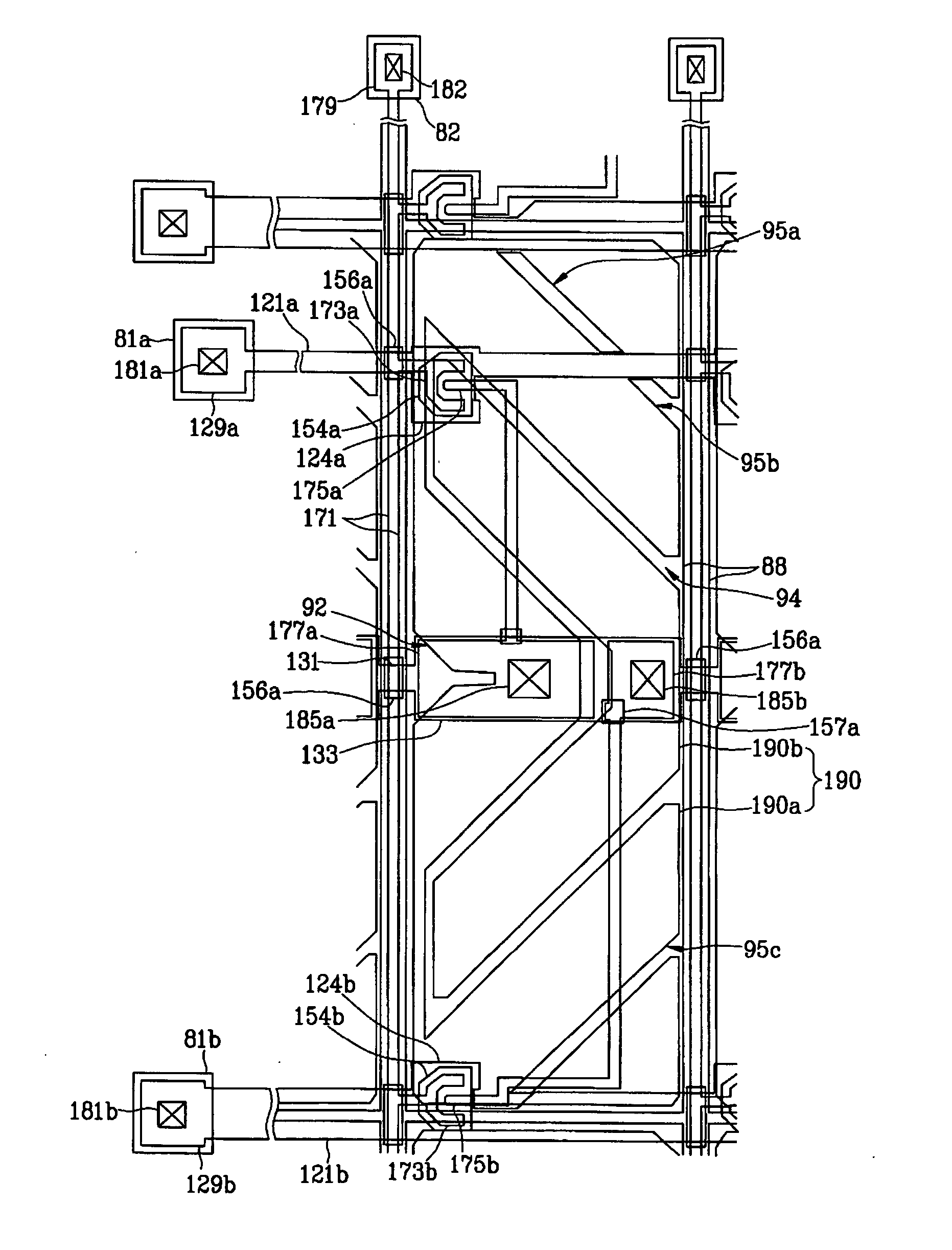
[0061] As shown in FIGS. 4 to 8, the LCD panel assembly includes a lower panel 100, an upper panel 200 facing the lower panel 100, and a liquid crystal layer 3 disposed between those panels.

[0062] The lower panel 100 will be specifically explained with reference to FIGS. 4, 6, 7 and 8.

[0063] Pairings of first and second gate lines 121a and 121b and a plurality of storage electrode lines 131 are formed on an insulating substrate 110 that may comprise transparent glass or plastic.

[0064] The first and second gate lines 121a and 121b extend (horizontally) parallel to each other, and are physically and electrically separated from each other, to transmit gate signals to the gates of TFTs in sub-pixels. The first and second gate lines 121a and 121b are arranged vertically. Each of the gate lines 121a has a plurality of first gate electrodes 124a and each of the gate lines 121b has a plurality of first gate electrodes 124b. The gate electrodes 124a and 124b protrude upward and downward. ...

second embodiment

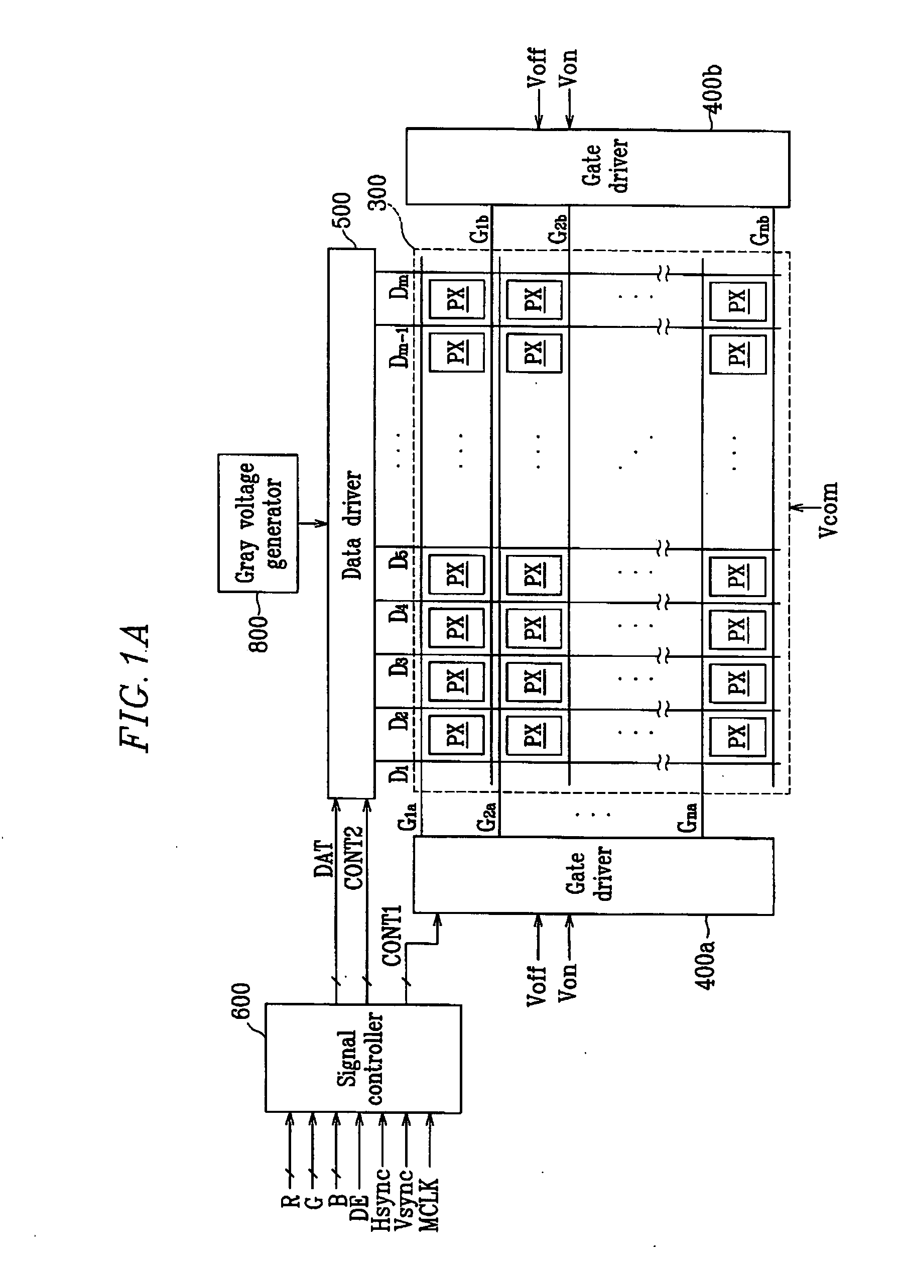
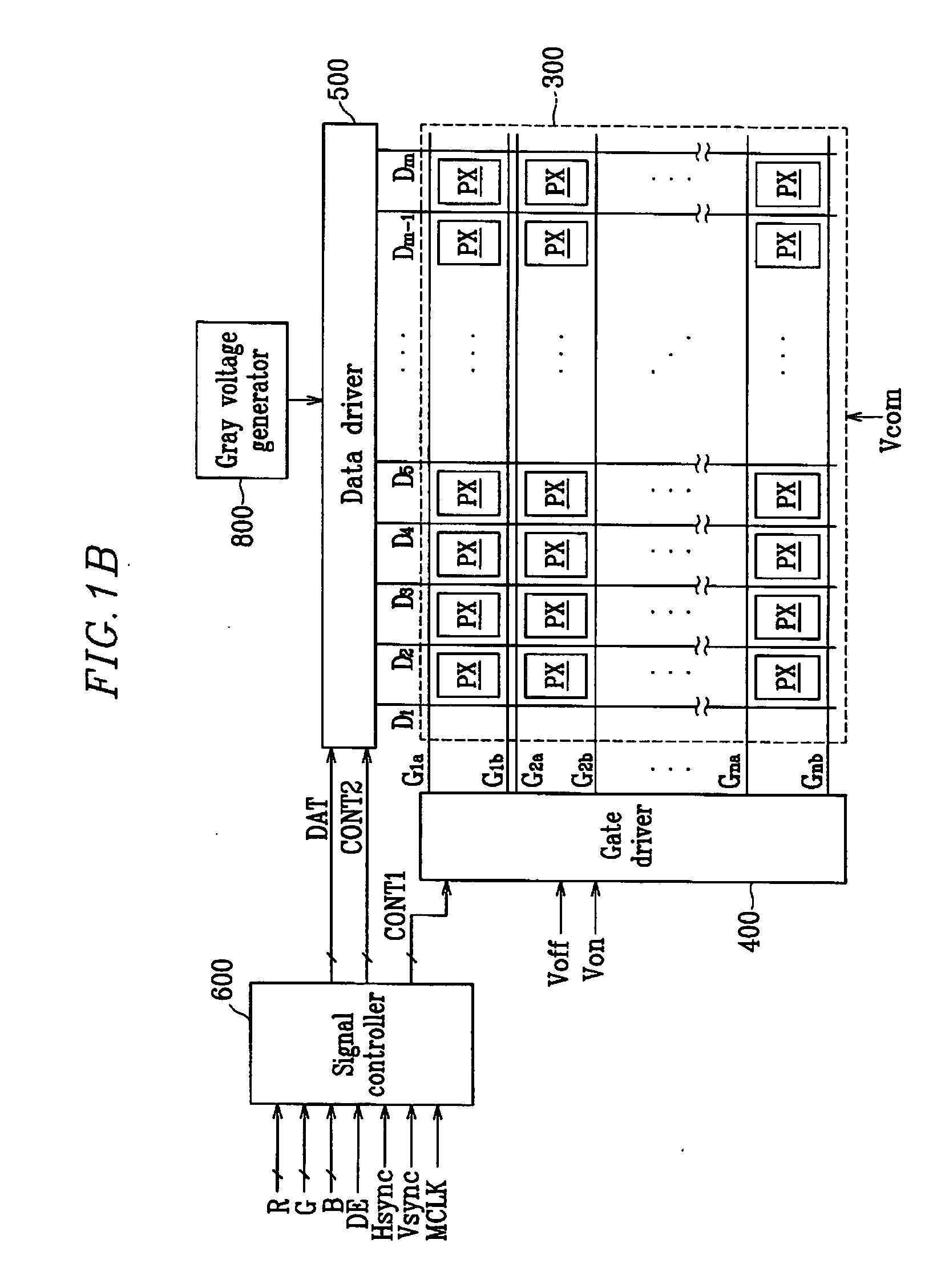
[0128] An LCD according to the present invention will now be specifically explained with reference to FIGS. 9 and 10.

[0129]FIG. 9 is a block diagram of an LCD according to the second embodiment of the present invention, and FIG. 10 is an equivalent circuit diagram of a pixel (PX) of the LCD of FIG. 9 according to the second embodiment of the present invention.

[0130] An LCD according to the second embodiment of the present invention includes a liquid crystal panel assembly 301, a gate driver 403 and a data driver 501 connected to the liquid crystal panel assembly 301, a gray voltage generator 801 connected to the data driver 501, and a signal controller 601 for controlling them.

[0131] The liquid crystal panel assembly 301 includes a plurality of display signal lines G1-Gn and D1-D2m, and a plurality (array) of pixels PX connected to those signal lines and arranged in the form of a matrix.

[0132] The display signal lines (G1-Gn and D1-D2m) include a plurality of gate lines G1-Gn for...

third embodiment

[0181] A pixel PX in an LCD according to the present invention will now be specifically described with reference to FIG. 13.

[0182]FIG. 13 is an equivalent circuit diagram of a pixel PX in a pixel array of an LCD according to a third embodiment of the present invention.

[0183]FIG. 13 illustrates display signal lines (GL, DL, Sla, SLb) and an equivalent circuit of two sub-pixels of one pixel PX. The display signal lines include a gate line indicated by GL, a data line indicated by DL, and a pair of first and second storage electrode lines SLa and SLb proceeding substantially parallel to the gate line GL.

[0184] The respective pixels PX include a pair of sub-pixels PXe and PXf. The sub-pixels PXe and PXf respectively include switching elements Qe and Qf connected to the gate and the data lines GL and DL, liquid crystal capacitors CLCe and CLCf connected to those switching elements, and storage capacitors CSTe and CSTf connected to the switching elements Qe and Qf and the storage electr...


PUM


Abstract

A liquid crystal display includes an array of pixels. Each pixel is divided into a first sub-pixel and a second sub-pixel, and different data voltages are separately applied to (or evolved at) the two sub-pixels, thereby enhancing the lateral side visibility. Each sub-pixel includes a sub-pixel electrode (connected to the drain electrode of a sub-pixel's switching element) overlapped with the sub-pixel's storage electrode. A first predetermined voltage is applied to the first sub-pixel and second predetermined voltage is applied the second sub-pixel, and thus the first sub-pixel electrode may receive a voltage lower than the voltage of the second sub-pixel electrode. The first sub-pixel electrode may be larger in area than the second sub-pixel electrode. The overlapping area between the first drain electrode and the storage electrode of a first sub-pixel may be larger than the overlapping area between the drain electrode and the storage electrode of a second sub-pixel. Thus the kickback voltage of the first sub-pixel may be substantially the same as the kickback voltage of the second sub-pixel.

Description

RELATED APPLICATION [0001] This application claims priority under 35 U.S.C. § 119 of Korean Patent Application No. 10-2005-0030678 filed on Apr. 13, 2005, the contents of which is incorporated by reference herein in its entirety. BACKGROUND OF THE INVENTION [0002] (1) Field of the Invention [0003] The present invention relates to a liquid crystal display. [0004] (2) Description of the Related Art [0005] A liquid crystal display (“LCD”), one of the most extensively used flat panel display devices, typically includes two substrates having field-generating electrodes (such as pixel and common electrodes) mounted thereon, and a liquid crystal layer sandwiched between the substrates. The LCD generates an electric field in the liquid crystal layer by applying voltages to the field-generating electrodes, and aligns the liquid crystal molecules of the liquid crystal layer to control the polarization of light incident thereto (e.g., from a “backlight”), thereby displaying the desired images....

Claims


Application Information

Patent Timeline
Patent Type & Authority Applications(United States)
IPC IPC(8): H01L29/04
CPCG02F1/136213G02F1/13624H01L27/124G02F1/136277H01L27/13G02F1/1343
Inventor KIM, DONG-GYU
Owner SAMSUNG DISPLAY CO LTD
Why Eureka
Try Eureka