Semiconductor device and manufacturing method thereof
- Summary
- Abstract
- Description
- Claims
- Application Information
AI Technical Summary
Benefits of technology
Problems solved by technology
Method used
Image

Examples
first embodiment
[0048] A semiconductor device and a manufacturing method thereof according to the first embodiment of the present invention will now be explained with reference to the drawings. In the present embodiment, the explanation will be given by employing an example of a diode as a semiconductor device.
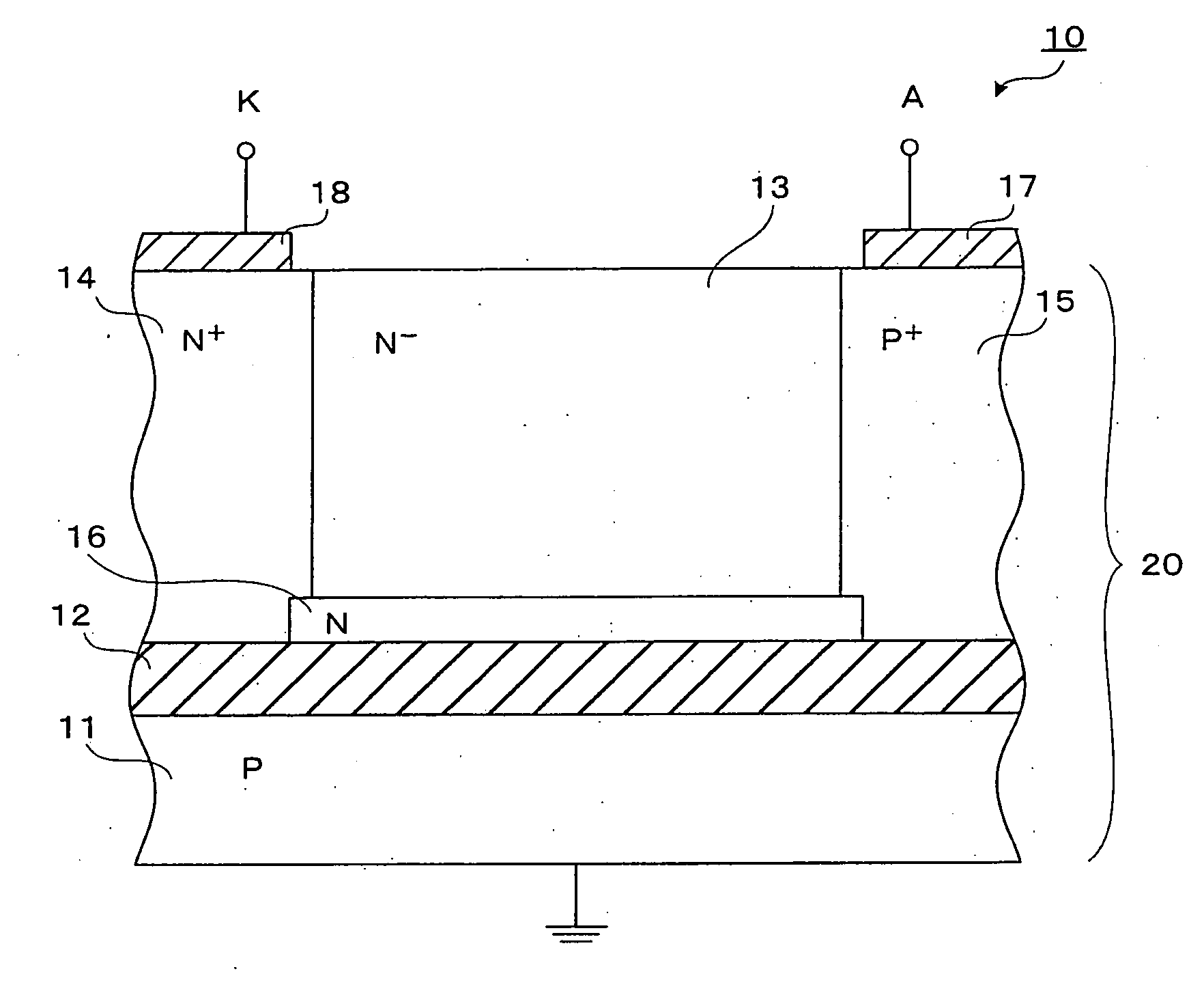
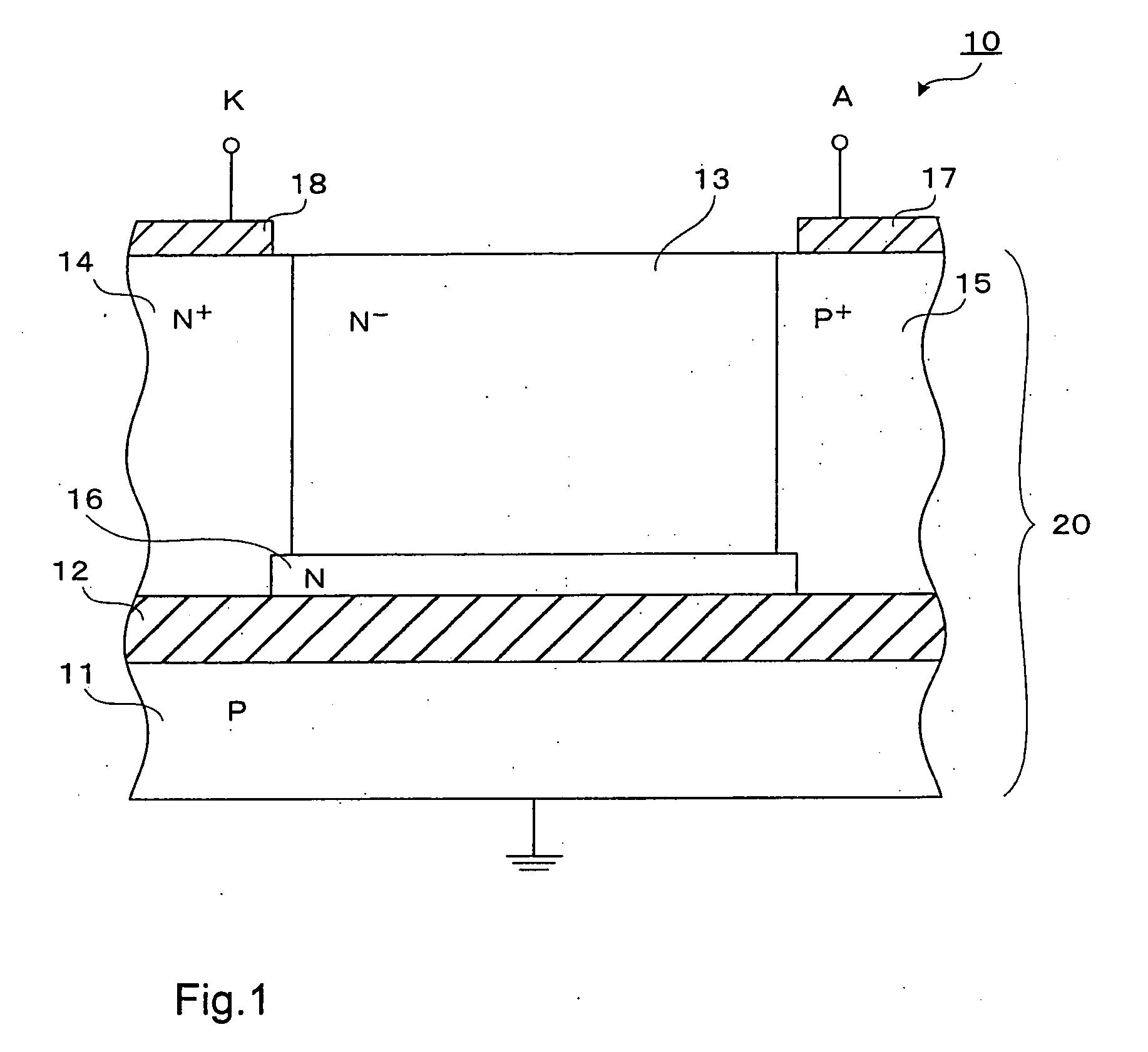
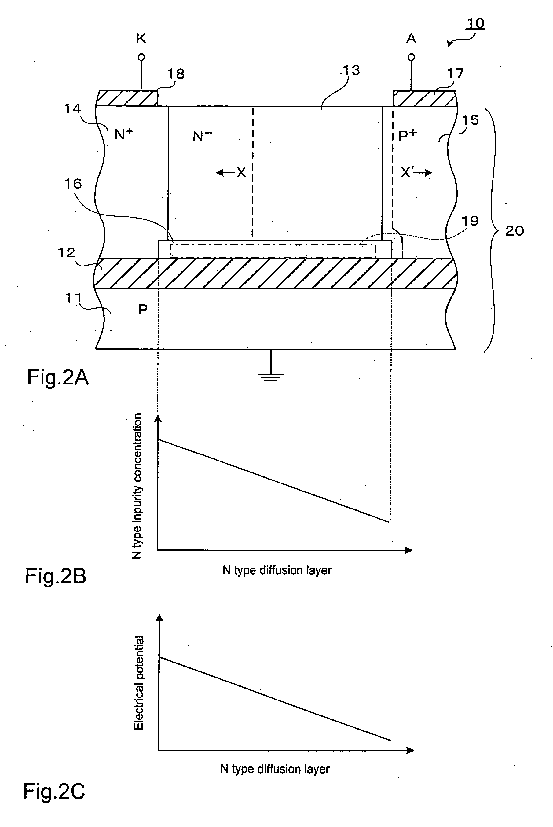
[0049] A semiconductor device 10 according to the first embodiment of the present invention is shown in FIG. 1 and FIG. 2A. FIG. 1 is a cross-sectional view of the semiconductor device 10. FIG. 2A is a cross-sectional view exemplarily showing the semiconductor device 10 in a state where a reverse-direction voltage is applied.
[0050] As shown in FIG. 1, the semiconductor device 10 comprises a semiconductor base 20, an anode electrode 17, and a cathode electrode 18.
[0051] The semiconductor base 20 comprises a P type semiconductor substrate 11, an insulating film 12, an N− type semiconductor region 13, an N+ type semiconductor region 14, a P+ type semiconductor region 15, and an N type diffusi...
second embodiment
[0082] A semiconductor device 30 according to the second embodiment of the present invention will now be explained with reference to the drawings. The present embodiment is different from the first embodiment in that the semiconductor device is not a diode, but a MOSFET (Metal Oxide Semiconductor Field Effect Transistor). Any parts that are common with the first embodiment will be given the same reference numerals as used in the first embodiment, and a detailed explanation for such parts will be omitted.
[0083] The semiconductor device 30 according to the second embodiment of the present invention is shown in FIG. 4. The semiconductor device 30 comprises a semiconductor base 39, a gate insulating film 35, a gate electrode 36, a drain electrode 37, and a source electrode 38.
[0084] The semiconductor base 39 comprises a P type semiconductor substrate 11, an insulating film 12, an N type diffusion layer 16, a drift region 31, a drain region 32, a base region 33, and a source region 34....
third embodiment
[0093] A semiconductor device according to the third embodiment of the present invention will now be explained with reference to the drawings. The present embodiment is different from the first embodiment in that the semiconductor device is an insulated gate bipolar transistor (hereinafter referred to as IGBT). Any parts that are common with the first embodiment will be given the same reference numerals as used in the first embodiment, and a detailed explanation for such parts will be omitted.
[0094] As shown in FIG. 5, a semiconductor device 40 comprises a semiconductor base 50, a collector electrode 46, a gate electrode 47, a gate insulating film 48, and an emitter electrode 49.
[0095] The semiconductor base 50 comprises a P type semiconductor substrate 11, an insulating film 12, an N type diffusion layer 16, an N− type base region 41, a P+ type collector region 42, a P+ type base region 43, an N+ type emitter region 44, and an N type buffer region 45.
[0096] The N− type base regi...
PUM
 Abstract
Description
Claims
Application Information
 - R&D
- Intellectual Property
- Life Sciences
- Materials
- Tech Scout
- Unparalleled Data Quality
- Higher Quality Content
- 60% Fewer Hallucinations
Browse by: Latest US Patents, China's latest patents, Technical Efficacy Thesaurus, Application Domain, Technology Topic, Popular Technical Reports.
© 2025 PatSnap. All rights reserved.Legal|Privacy policy|Modern Slavery Act Transparency Statement|Sitemap|About US| Contact US: help@patsnap.com