Dual conversion gain pixel using Schottky and ohmic contacts to the floating diffusion region and methods of fabrication and operation

a gain pixel and ohmic contact technology, applied in the field of dual conversion gain imaging devices, can solve the problems of excess charge overflow, transfer of charge into the substrate and adjacent pixels, etc., and achieve the effect of improving the dynamic rang

Active Publication Date: 2006-10-19
APTINA IMAGING CORP
View PDF23 Cites 48 Cited by
  • Summary
  • Abstract
  • Description
  • Claims
  • Application Information

AI Technical Summary

Benefits of technology

[0014] The present invention in the exemplary embodiments provides an imager with dual conversion gain charge storage and thus, improved dynamic range. A dual conversion gain element (e.g., Schottky diode) is coupled between a floating diffusion region and a respective c

Problems solved by technology

When the light captured and converted into charge by the photosensor 12 is greater than the capacity of the photosens

Method used


Image

  • Dual conversion gain pixel using Schottky and ohmic contacts to the floating diffusion region and methods of fabrication and operation
  • Dual conversion gain pixel using Schottky and ohmic contacts to the floating diffusion region and methods of fabrication and operation
  • Dual conversion gain pixel using Schottky and ohmic contacts to the floating diffusion region and methods of fabrication and operation

Examples


Embodiment Construction

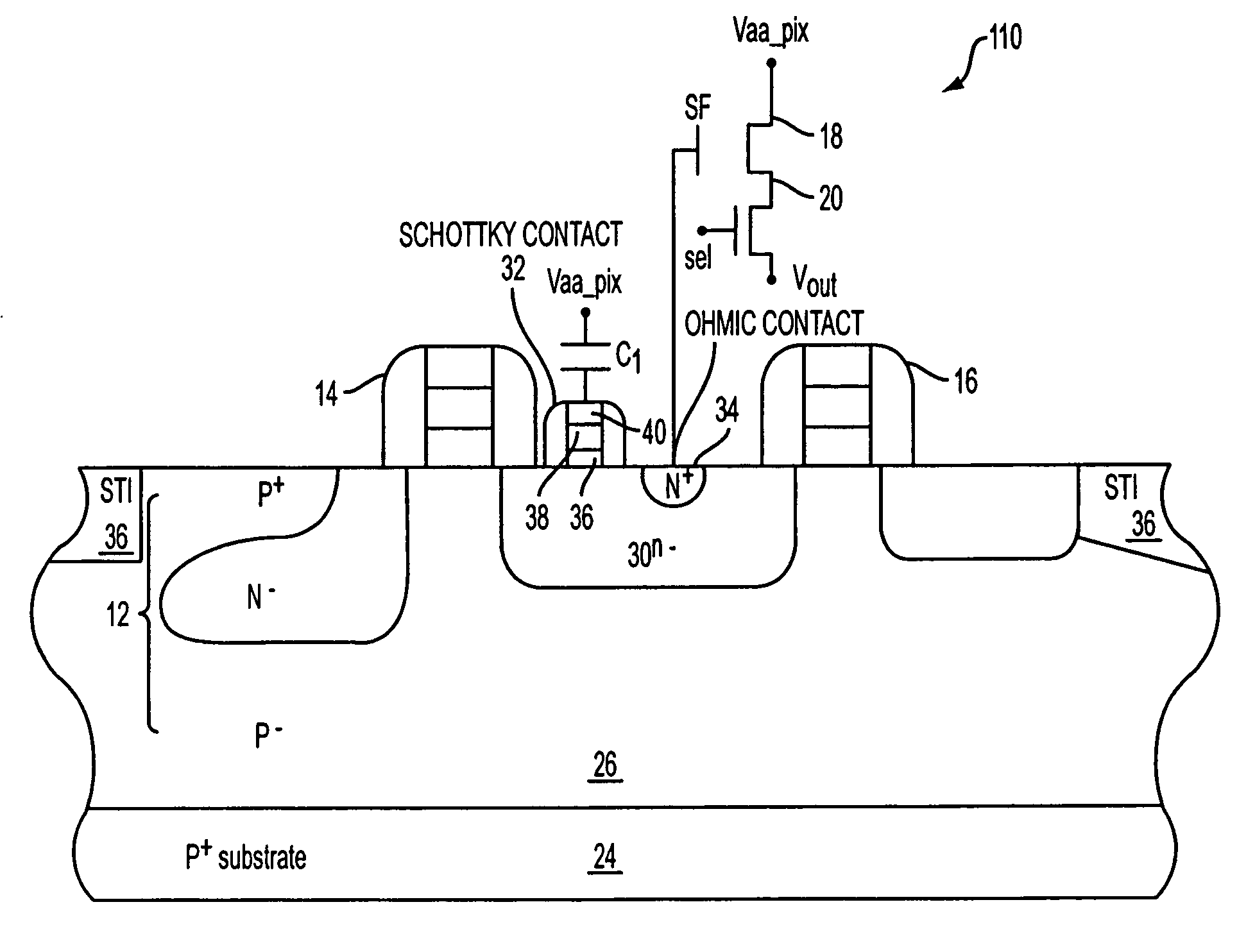
[0026] In the following detailed description, reference is made to the accompanying drawings which form a part hereof, and in which is shown by way of illustration specific embodiments in which the invention may be practiced. These embodiments are described in sufficient detail to enable those skilled in the art to practice the invention, and it is to be understood that other embodiments may be utilized, and that structural, logical and electrical changes may be made without departing from the spirit and scope of the present invention.

[0027] The term “substrate” is to be understood as a semiconductor-based material including silicon, silicon-on-insulator (SOI) or silicon-on-sapphire (SOS) technology, doped and undoped semiconductors, epitaxial layers of silicon supported by a base semiconductor foundation, and other semiconductor structures. Furthermore, when reference is made to a “substrate” in the following description, previous process steps may have been utilized to form regio...


PUM


Abstract

The exemplary embodiments provide an imager with dual conversion gain charge storage and thus, improved dynamic range. A dual conversion gain element (e.g., Schottky diode) is coupled between a floating diffusion region and a respective capacitor. The dual conversion gain element switches in the capacitance of the capacitor, in response to charge stored at the floating diffusion region, to change the conversion gain of the floating diffusion region from a first conversion gain to a second conversion gain. In an additional aspect, the exemplary embodiments provide an ohmic contact between the gate of a source follower transistor and the floating diffusion region which assists in the readout of the dual conversion gain output signal of a pixel.

Description

FIELD OF THE INVENTION [0001] The invention relates generally to imaging devices and more particularly to dual conversion gain imaging devices. BACKGROUND OF THE INVENTION [0002] Imaging devices, including charge coupled devices (CCD) and complementary metal oxide semiconductor (CMOS) imagers, are commonly used in photo-imaging applications. [0003] A CMOS imager circuit includes a focal plane array of pixels, each of the pixels including a photosensor, for example, a photogate, photoconductor or a photodiode for accumulating photo-generated charge a portion of the substrate. Each pixel has a charge storage region, formed on or in the substrate, which is connected to the gate of an output transistor that is part of a readout circuit. The charge storage region may be constructed as a floating diffusion region. In some imager circuits, each pixel may include at least one electronic device such as a transistor for transferring charge from the photosensor to the storage region and one de...

Claims


Application Information

Patent Timeline
IPC IPC(8): H01L31/062
CPCH01L27/14609H01L27/14641H01L27/14654H04N25/59H01L27/14H01L29/872
Inventor PATRICK, INNAHONG, SUNGKWON C.MCKEE, JEFFREY A.
Owner APTINA IMAGING CORP
Why Eureka
Try Eureka