Unlock instant, AI-driven research and patent intelligence for your innovation.

Integrated circuit system for bonding

a circuit system and integrated circuit technology, applied in the field of semiconductor technology, can solve the problems of insufficient temperature control capability of sputtering the relatively thick ubm metal layer, difficulty in soldering and undesirable materials,

Active Publication Date: 2006-10-19
JCET SEMICON (SHAOXING) CO LTD
View PDF13 Cites 12 Cited by
  • Summary
  • Abstract
  • Description
  • Claims
  • Application Information

AI Technical Summary

Benefits of technology

The present invention provides an integrated circuit system with a precursor for wire bond and flip chip structures. The precursor has multiple contact pads and a layer of titanium is deposited on top. A layer of nickel-vanadium is then deposited on top of the titanium layer. A layer of copper is deposited on top of the nickel-vanadium layer. A mask is formed on at least a portion of the copper layer, and the unmasked portions of the layers are removed to expose the titanium layer. The exposed titanium layer is then etched using an etching solution containing an etchant, a viscosity modifier, and an oxidizer. The technical effect of this invention is to provide a reliable and efficient method for creating integrated circuit structures with multiple contact pads and exposed titanium layers for wire bonding.

Problems solved by technology

In contrast, the wire bond technique is a perimeter method only, and is therefore more limited.
While techniques have been tried for soldering directly to the Al pads of the underlying integrated circuit, it is well known and accepted that Al is a difficult and undesirable material for soldering.
Unfortunately, some sputtering tools do not have sufficient temperature control capability for sputtering the relatively thick UBM metal layers.
In addition, the lift-off method is often not cost effective.
However, the etch-back process has certain limitations as well.
One such limitation is selectivity.
In the case of UBM structures formed of Ti / NiV / Cu, the wet etching of the Ti / NiV / Cu layers is not a problem with respect to the UBM layers, but it is a problem with respect to exposed Al wire-bonding pads due to possible poor selectivity, particularly during the Ti etching phase.
However, dry etching of Ti contaminates the process chamber quickly and attacks the polyimide surface of the passivation layer.
As a consequence, if the sputtering tool is not capable of supporting the lift-off technique, the wet etching of the Ti is usually the only reasonable option.
Consequently, common Ti etchants such as this typically have poor selectivity over Al, typically over 1:10 (Ti: Al).
During the etching of the Ti, the Al wire-bonding pads can therefore be seriously attacked, to the extent that they become disconnected from their circuits in the die.
Another problem with respect to such wet etching with HF is that the presence of Cu and NiV in the etching process causes a residue of Ti to be left on the polyimide surface.
Still another problem with respect to wet etching is endpoint detection for the etching process.
This makes it hard to detect the endpoint of the entire process because the sudden disappearance of the Ti layer does not mean that the Ti on the underlying passivation layer has been cleared or removed.
Solutions to these problems have been long sought but prior developments have not taught or suggested any solutions and, thus, solutions to these problems have long eluded those skilled in the art.

Method used


Image

  • Integrated circuit system for bonding
  • Integrated circuit system for bonding
  • Integrated circuit system for bonding

Examples


Embodiment Construction

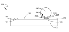
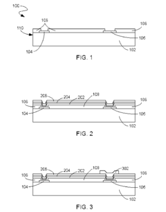
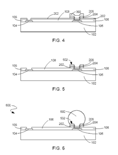
[0027] The following embodiments are described in sufficient detail to enable those skilled in the art to make and use the invention, and it is to be understood that other embodiments would be evident based on the present disclosure and that process or mechanical changes may be made without departing from the scope of the present invention.

[0028] In the following description, numerous specific details are given to provide a thorough understanding of the invention. However, it will be apparent that the invention may be practiced without these specific details. In order to avoid obscuring the present invention, some well-known system configurations and process steps are not disclosed in detail. Likewise, the drawings showing embodiments of the invention are semi-diagrammatic and not to scale and, particularly, some of the dimensions are for the clarity of presentation and are shown exaggerated in the drawing FIGs. Also, where multiple embodiments are disclosed and described having so...


PUM

PropertyMeasurementUnit
thicknessaaaaaaaaaa
viscosityaaaaaaaaaa
thicknessaaaaaaaaaa

Abstract

An integrated circuit system provides a precursor for an integrated wire bond and flip chip structure. The precursor has a plurality of contact pads thereon. A layer of titanium is deposited on the precursor. A layer of nickel-vanadium is deposited on the layer of titanium. A layer of copper is deposited on the layer of nickel-vanadium. A mask is formed on at least a portion of the layer of copper. Portions of the layers of copper and nickel-vanadium not protected by the mask are removed to expose portions of the layer of titanium. The exposed portions of the layer of titanium are etched with an etching solution consisting of an etchant, a viscosity modifier, and an oxidizer.

Description

TECHNICAL FIELD [0001] The present invention relates generally to semiconductor technology, and more particularly to integrated circuit systems for bonding having wire bond and solder bump metallization and patterning for wafer level packages. BACKGROUND ART [0002] In the manufacture and assembly of electronic devices, two high-density interconnection techniques—wire bond and flip chip—are commonly used to mount and electrically connect semiconductor dies (or “chips”) on interconnection substrates. The wire bond technique presents wire bond pads (typically formed from aluminum (“Al”)) on the substrate surface. The flip chip technique presents solder pads (typically formed as solder balls) on the substrate surface. [0003] Flip chip interconnections provide the shortest electrical connecting paths, and therefore the highest electrical performance and speed. Flip chip interconnections also accommodate the greatest number of chips and chip connections within a given space because the fl...

Claims


Application Information

Patent Timeline
Patent Type & Authority Applications(United States)
IPC IPC(8): H01L23/48H01L23/52H01L29/40
CPCC23F1/26H01L2224/45144H01L24/11H01L2224/0401H01L2224/131H01L2924/01013H01L2924/01014H01L2924/01022H01L2924/01027H01L2924/01028H01L2924/01029H01L2924/01079H01L2924/014H01L2924/05042H01L2924/14H01L2924/30107H01L2924/00014H01L2224/45124H01L2924/00013H01L2924/01023H01L2924/01033H01L2924/01072H01L24/02H01L2224/13099H01L2924/00H01L2224/48H01L24/03H01L24/05H01L24/13
Inventor LIN, YAOJIANDO, BYUNG TAILOOI, WAN LAYCAO, HAIJING
Owner JCET SEMICON (SHAOXING) CO LTD