Color filter array panel, liquid crystal display having the same, and manufacturing method thereof

a technology of liquid crystal display and color filter array, which is applied in the direction of photomechanical treatment originals, instruments, coatings, etc., can solve the problems of step difference and easy defect of liquid crystal molecules alignmen

Inactive Publication Date: 2006-10-19
SAMSUNG DISPLAY CO LTD
View PDF9 Cites 19 Cited by
  • Summary
  • Abstract
  • Description
  • Claims
  • Application Information

AI Technical Summary

Benefits of technology

[0022] In the above aspect of the present invention, the second common electrode may have cut portions that are formed at positions corresponding to the transparent organic layers, and the area of each transparent organic layer may be 1% to 90% of the area of each reflective electrode.

Problems solved by technology

However, in the case where there is a patterned layer including patterned portions and non-patterned portions under the color filters, a step difference may occur at interface portions therebetween during the formation of the photosensitive film.
However, in this case, defects in the alignment of liquid crystal molecules may easily occur due to the step difference caused by the light holes.

Method used


Image

  • Color filter array panel, liquid crystal display having the same, and manufacturing method thereof
  • Color filter array panel, liquid crystal display having the same, and manufacturing method thereof
  • Color filter array panel, liquid crystal display having the same, and manufacturing method thereof

Examples


first embodiment

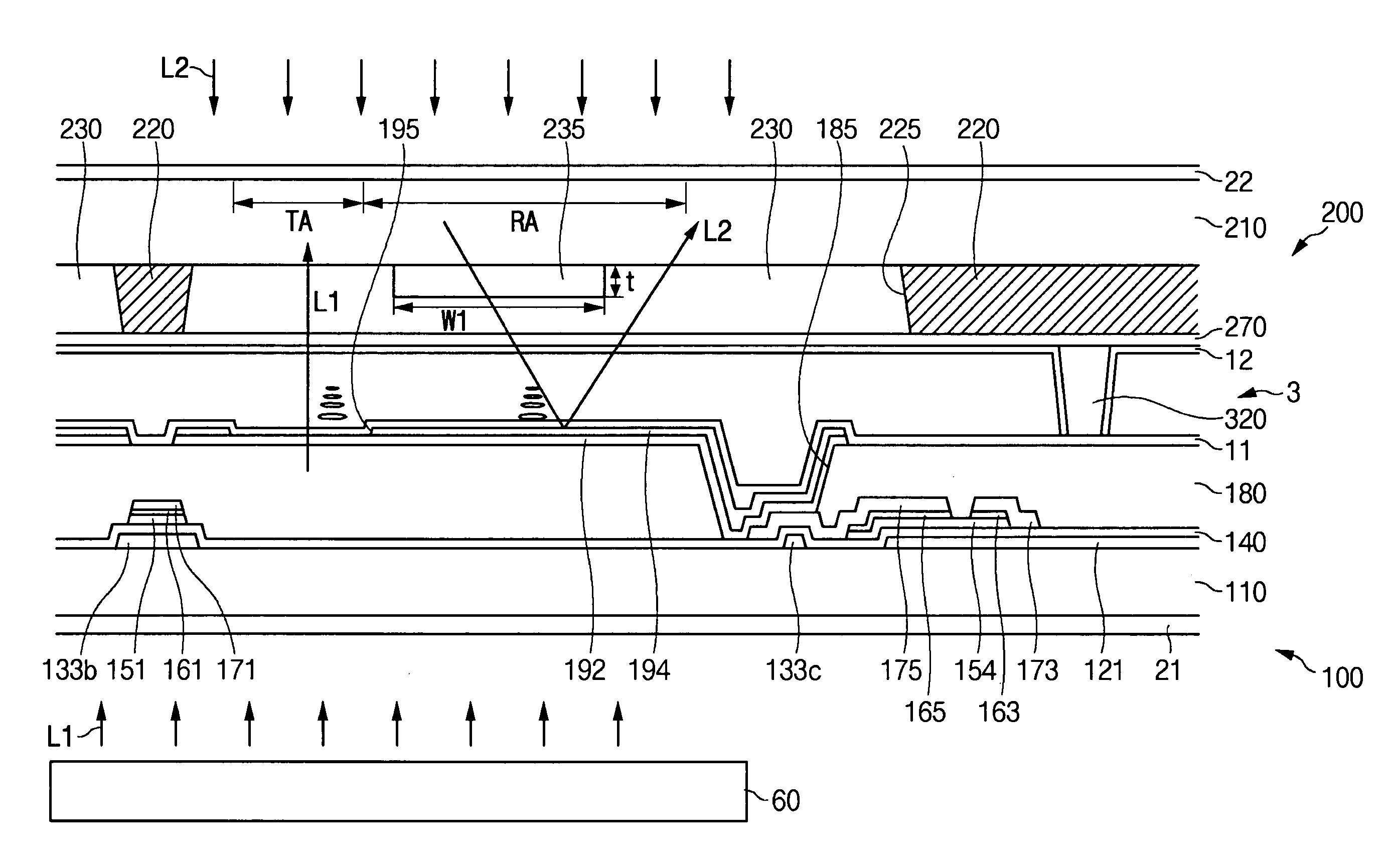
[0041] The LCD includes a transistor array panel 100, a color filter array panel 200, and a liquid crystal layer 3 interposed between the two panels 100 and 200.

[0042] Firstly, the transistor array panel 100 will be described in detail with reference to FIG. 1 and FIGS. 3 to 5.

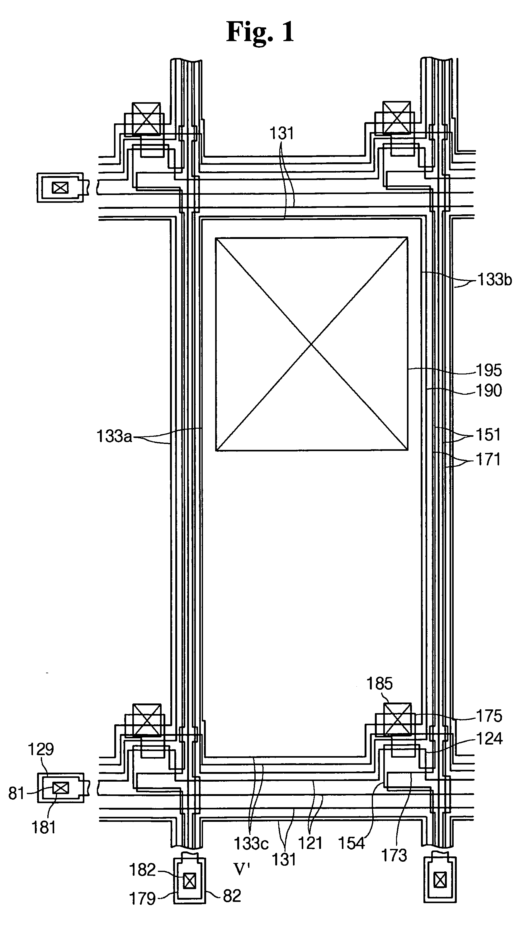
[0043] A plurality of gate lines 121 and a plurality of storage electrode lines 131 are disposed on an insulating substrate 110 made of a transparent glass or plastic material.

[0044] The gate lines 121 for transmitting gate signals mainly extend in the transverse direction.

[0045] The gate lines 121 include a plurality of gate electrodes 124 that protrude upwardly, and end portions 129 that have wide areas for connection to other layers or external driver circuits. A gate driver circuit (not shown) that generates the gate signals may be mounted on a flexible printed circuit film attached to the substrate 110. Alternatively, the gate driver circuit may be directly mounted on the substrate 110, or it may be i...

second embodiment

[0105] Now, an LCD according to the present invention will be described in detail with reference to the cross-sectional view of FIG. 10.

[0106] As shown in FIG. 10, the LCD according to the second embodiment is different from the LCD shown in FIG. 4 according to the first embodiment in that convex-shaped members 235a are formed on surfaces of the transparent organic layers 235.

[0107] According to the second embodiment, after the ink 5 for the color filters 230 is sprayed by using the inkjet printing system, the ink 5 can easily flow over the substrate 210 without remaining on the transparent organic layers 235, so that the color filters 230 can be planarized.

[0108] When the transparent organic layers 235 have a flat surface, the ink 5 may tend to puddle more on the transparent organic layers 235, so the levels of the color filters 230 formed on the transparent organic layers 235 may be higher than the levels of the color filters 230 formed on regions where the transparent organic l...

third embodiment

[0109] Now, an LCD according to the present invention will be described in detail with reference to the cross-sectional view of FIG. 11.

[0110] As shown in FIG. 11, in the LCD according to the third embodiment of the present invention, light-blocking members 220 and transparent organic layers 235 are formed on a substrate 210, and a first common electrode 271 is formed on the substrate 210, the light-blocking members 220, and the transparent organic layers 235.

[0111] By using an inkjet printing system, color filters 230 are formed within openings 225 between the light-blocking members 220. Some portions of the first common electrode 271 corresponding to the openings 225 are covered with the color filters 230, and other portions of the first common electrode 271 are not covered with the color filters 230.

[0112] A second common electrode 272 is formed on the color filters 230 and the exposed portions of the first common electrode 271. Portions 272a are cut from regions of the second ...


PUM

PropertyMeasurementUnit
transparentaaaaaaaaaa
slant angleaaaaaaaaaa

Abstract

A method of manufacturing a color filter array panel is provided. The method includes forming light-blocking members having a plurality of openings on a substrate, forming transparent organic layers within the openings, forming color filters by spraying ink for the color filters in the openings, and forming a common electrode on the color filters and the light-blocking members. The transparent organic layers are formed in reflective areas, and the color filters are formed by using an inkjet printing system so that it is possible to planarize the color filters and improve color characteristics of the reflective areas.

Description

[0001] This application claims priority to Korean Patent Application No. 2005-0030673, filed on Apr. 13, 2005, and all the benefits accruing therefrom under 35 U.S.C. §119, and the contents of which in its entirety are herein incorporated by reference. BACKGROUND OF THE INVENTION [0002] (a) Field of the Invention [0003] The present invention relates to a color filter array panel, a liquid crystal display having the color filter array panel, and a method of manufacturing the color filter array panel. [0004] (b) Description of the Related Art [0005] A liquid crystal display (LCD), which is one of the most widely used flat panel display apparatuses, includes two panels having electric field generating electrodes such as pixel electrodes and a common electrode, and a liquid crystal layer interposed therebetween. The LCD displays an image by applying a voltage to the electric field generating electrodes, which generates an electric field in the liquid crystal layer to determine alignment...

Claims


Application Information

Patent Timeline
Patent Type & Authority Applications(United States)
IPC IPC(8): G02F1/1335
CPCG02F1/133512G02F2201/48G02F1/133555G02F1/133516E03C1/2302
Inventor RHO, SOO-GUY
Owner SAMSUNG DISPLAY CO LTD
Why Eureka
Try Eureka