Defect inspection apparatus, defect inspection method and method of inspecting hole pattern

a technology of defect inspection and inspection apparatus, which is applied in the field of defect inspection method and inspection method of hole pattern inspection, can solve the problems of deterioration of s/n ratio, affecting the underlying layer, and reducing the information on the pattern of the uppermost layer that is to be primarily inspected, so as to reduce background noise, inspection of hole pattern, and good s/n ratio

Active Publication Date: 2006-10-19
NIKON CORP
View PDF10 Cites 41 Cited by
  • Summary
  • Abstract
  • Description
  • Claims
  • Application Information

AI Technical Summary

Benefits of technology

[0030] Generally, hole patters such as contact holes are very small, and it is impossible for conventional inspection methods to inspect them reliably. With the method according to the tenth aspect of the invention, it is possible to reduce background noise, and inspection of hole pa

Problems solved by technology

Consequently, when the influence of the pattern of the underlying layer is significantly large, it constitutes a noise and information on the pattern of the uppermost layer that is to be primarily inspected is relatively decreased, so that a problem of deterioration of the S/N ratio arises.
Especially, a hole pattern such as a contact hole pattern

Method used


Image

  • Defect inspection apparatus, defect inspection method and method of inspecting hole pattern
  • Defect inspection apparatus, defect inspection method and method of inspecting hole pattern
  • Defect inspection apparatus, defect inspection method and method of inspecting hole pattern

Examples


first embodiment

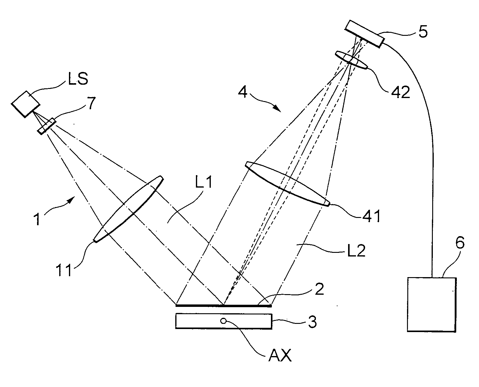
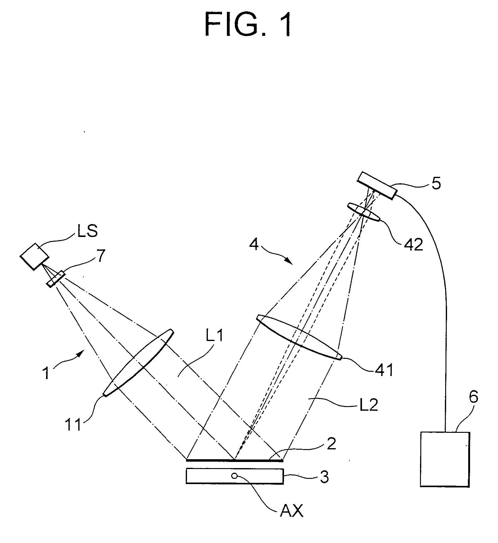
[0039] In the following, embodiments of the present invention will be described with reference to the accompanying drawings. FIG. 1 schematically shows a defect inspection apparatus according to the present invention. In this apparatus, illumination light L1 emitted from a lamp house LS is converted into substantially parallel light by a lens 11 that constitutes an illumination optical system 1 to illuminate a wafer 2 placed on a stage 3. In the interior of the lamp house LS, there is provided a light source such as a halogen lamp, a metal halide lamp or the like and a wavelength selective filter, so that light within only a limited wavelength range is picked up for use as the illumination light L1.

[0040] A polarizing plate 7 is disposed in the vicinity of light emitting portion of the lamp house LS to convert the illumination light L1 emitted from the lamp house into linearly polarized light. The polarizing plate 7 is rotatable about the optical axis of the illumination optical sys...

second embodiment

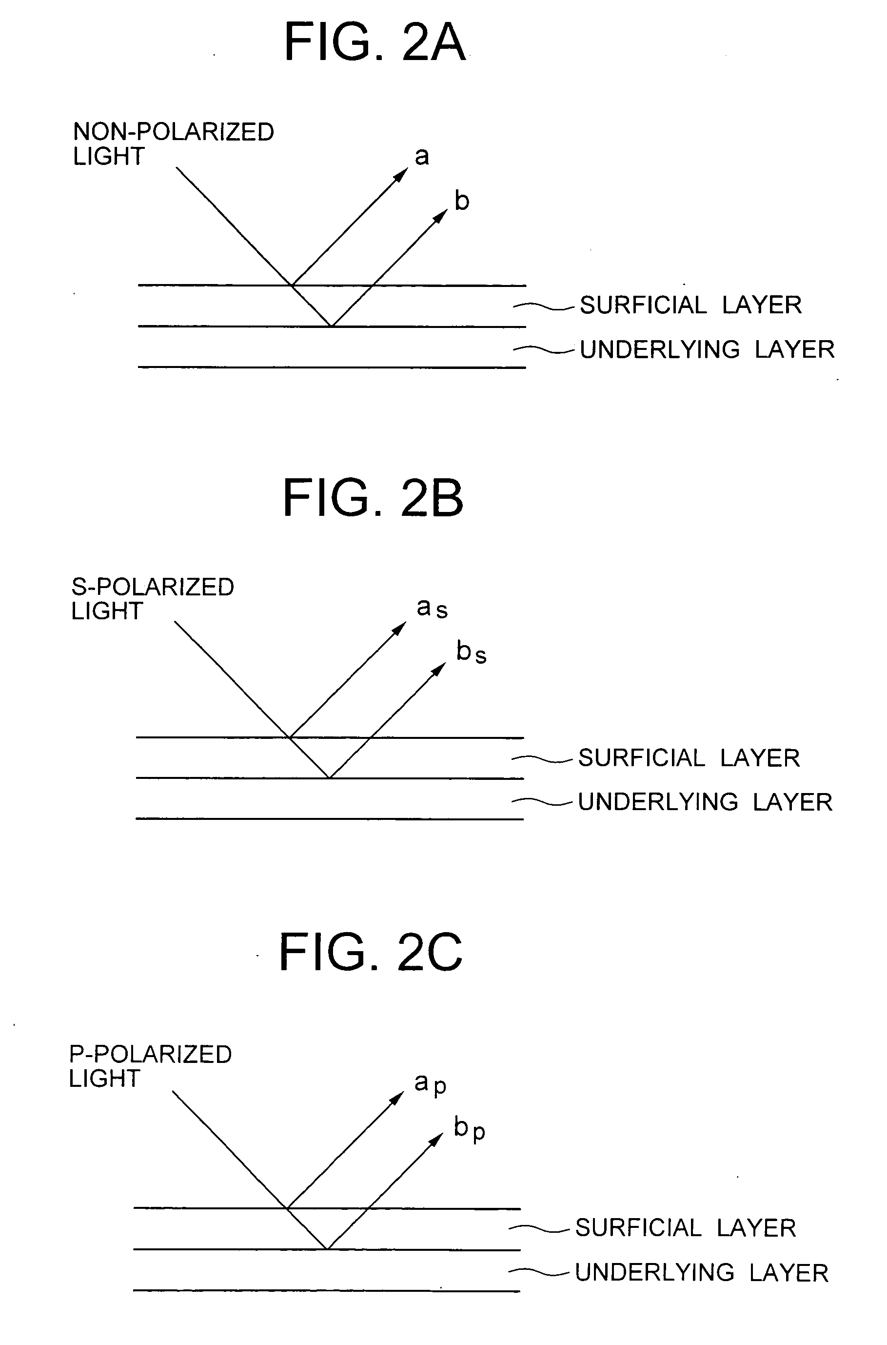
[0054] The inventors found the fact that in the defect inspection apparatus inspection of a hole pattern can be especially effectively performed when the wafer 2 is illuminated by linearly polarized illumination light (preferably, by illumination light having a polarization state for which the reflectance at the substrate surface is high as described before) and the polarizing plates 7 and 8 are adjusted in such a way that such linearly polarized light included in the diffracted light from the wafer that oscillates in the direction orthogonal to the illumination light L2 is picked up, namely in such a way that a state of so-called crossed Nicols is established.

[0055] Although the crossed Nicols normally renders the image field dark, areas in which hole patterns were formed could be picked up as images. This can be explained as follows. When linearly polarized light is incident on a sample, the polarization state of the light is changed when reflected and diffracted at the surface o...


PUM


Abstract

A defect inspection apparatus for inspecting a defect of a substrate as an object to be inspected comprises an illumination optical system for illuminating the substrate, a receiving optical system for receiving diffracted light from the substrate and a polarizing element provided in either one of the illumination optical system or the receiving optical system.

Description

[0001] This is a Continuation-in-Part of application Ser. No. 10 / 805,240 filed Mar. 22, 2004. The entire disclosure of the prior application is hereby incorporated by reference herein in its entirety. This application claims the benefit of Japanese Patent application Nos. 2003-085185 and 2004-322905 which are hereby incorporated by reference.BACKGROUND OF THE INVENTION [0002] 1. Field of the Invention [0003] The present invention relates to a defect inspection apparatus and a defect inspection method for detecting defects such as surface irregularities or dents etc. on a substrate for use, for example, in a process of manufacturing semiconductor devices or the like. The present invention also relates to a method of inspecting a hole pattern such as a contact hole or the like. [0004] 2. Related Background Art [0005] In the manufacturing of a semiconductor device or liquid crystal substrate, various different circuit patterns are formed repeatedly in many layers. A process for forming...

Claims


Application Information

Patent Timeline
IPC IPC(8): G01N21/88
CPCG01N21/95692
Inventor SUGIHARA, MARIOOMORI, TAKEOFUKAZAWA, KAZUHIKO
Owner NIKON CORP
Why Eureka
Try Eureka