Method for producing structure

a technology of structure and method, applied in the field of microstructure, can solve the problems of requiring a long time of several hours, affecting the quality of anodized layer, and the ineffective use of anodized layer, and achieve the effects of reducing time, low surface roughness, and high gloss

Inactive Publication Date: 2006-10-19
FUJIFILM CORP +1
View PDF3 Cites 53 Cited by
  • Summary
  • Abstract
  • Description
  • Claims
  • Application Information

AI Technical Summary

Benefits of technology

[0070] The structure production method according to aspect (I) of the present invention is capable of producing a structure having regularly arranged recesses in a reduced time.
[0071] The nanostructure production method according to aspect (II) of the present invention is capable of producing a nanostructure comprising an anodized layer, in which a low surface roughness and a high glossiness are attained, and accordingly, an improved S / N ratio is realized when the structure is used for an optical device or a magnetic device.
[0072] The nanostructure production method according to aspect (II) of the present invention is a method for producing a nanostructure having micropores made by anodization or anodic formation, wherein the anodization is conducted after mirror finishing the surface of a high purity aluminum plate by removing visually recognizable defects generated on the surface, such as “blisters” and rolling streaks, to thereby improve smoothness of the surface of the anodized nanostructure. In consequence, a structure which is ordered over a large area and applicable to an electromagnetic device such as optical device or magnetic device can be obtained in a simple procedure.

Problems solved by technology

However, the layer removal step using the mixed aqueous solution of chromic acid and phosphoric acid as described above generally required a long time of several hours to well over ten hours although the time required may vary with the thickness of the anodized layer.
In addition, the anodized layer could not be effectively used because of the dissolution.
The anodized layer produced under anodizing conditions described in JP 61-88495 A had an excessively large coefficient of variation in the pore diameter, and could not be used as a sample stage for Raman spectroscopic analysis, or the like.
When the thickness of the layer is reduced by the current recovery method described in JP 61-88495 A, the regularly arranged recesses on the surface of the aluminum member were lost and the coefficient of variation in the pore diameter was too large, and the aluminum member could not be used as a sample stage for Raman spectroscopic analysis, or the like.

Method used


Image

  • Method for producing structure
  • Method for producing structure

Examples


examples

[0407] Next, the present invention is described in more detail with reference to Examples relating to aspect (I) of the present invention. However, aspect (I) of the present invention is not limited to such Examples.

1. Production of Structure

examples 1 to 10

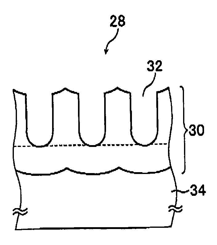
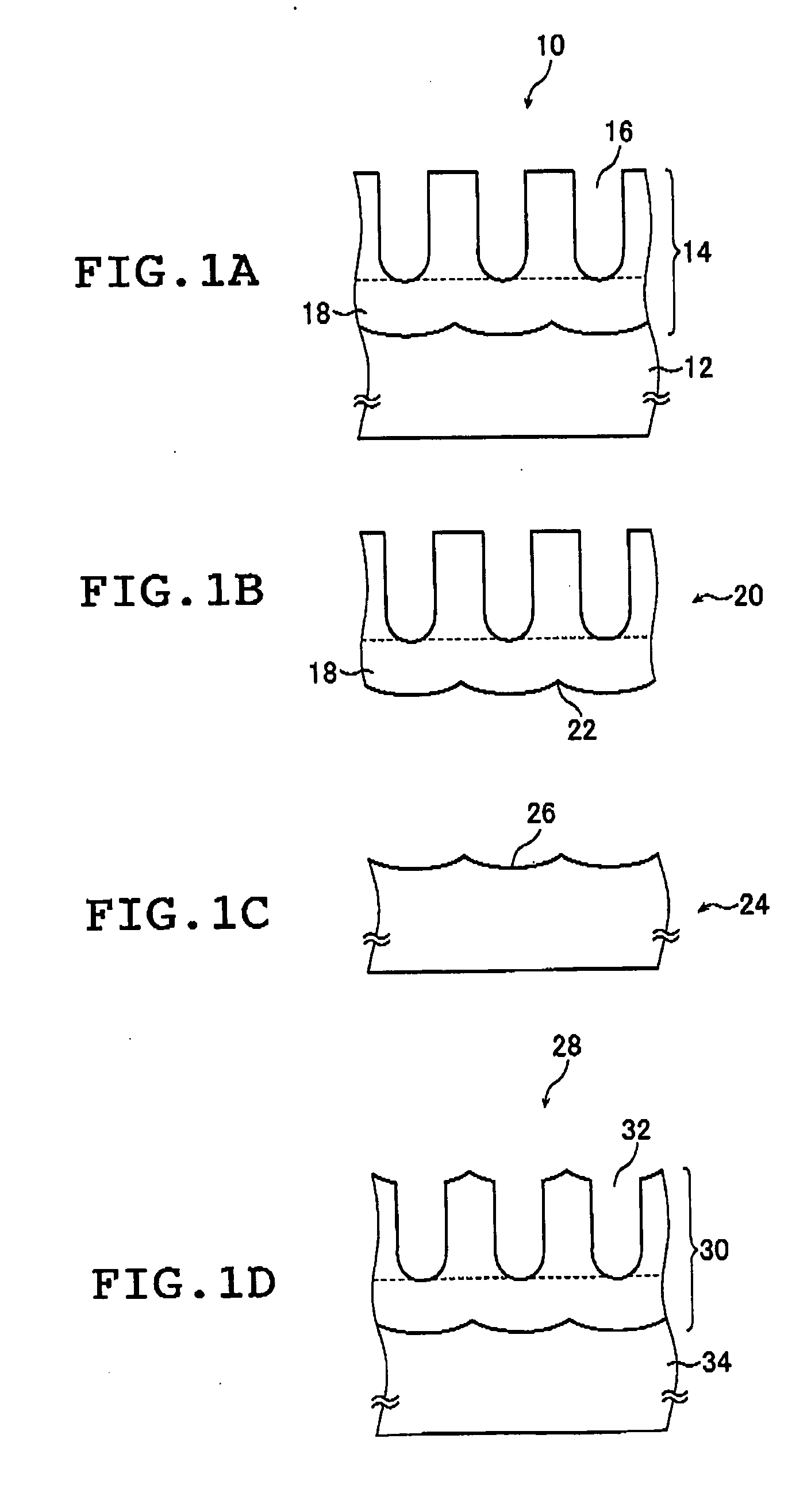
[0408] An aluminum substrate was subjected to a mirror finishing treatment, a self-ordering anodizing treatment, and a reverse electrolysis in this order to obtain a structure composed of an anodized layer, and the substrate. The resulting aluminum substrate was subjected to a main anodizing treatment, a pore widening treatment, a sealing treatment, a surface treatment, and an electrodeposition in this order to thereby obtain a structure composed of the aluminum substrate having micropores which are sealed with a metal.

[0409] Each treatment will be described below in more detail.

(1) Substrate

[0410] The following substrate was used for the production of the structures.

[0411] Substrate: a high purity aluminum available from Wako Pure Chemical Industries, Ltd. having an aluminum purity of 99.99 wt % and a thickness of 0.4 mm.

(2) Mirror Finishing Treatment

[0412] The substrate was subjected to the following mirror finishing treatment.

[0413] The mirror finishing treatment was con...

examples 11 and 12

[0437] In these Examples, the aluminum substrates used were substrate 7 and substrate 10 used in the Examples corresponding to aspect (II) of the present invention as described later. The substrate was subjected sequentially to the self-ordering anodizing treatment and the reverse electrolysis as described below to obtain a structure composed of an anodized layer and the substrate as left. The thus obtained aluminum substrate was further subjected to the main anodizing treatment, the pore widening treatment, the sealing treatment, the surface treatment, and the electrodeposition treatment in this order to produce a structure composed of the aluminum substrate having the micropores sealed with a metal. The substrate used in Example 11 was substrate 7, and the substrate used in Example 12 was substrate 10.

[0438] The treatments are described in detail.

(1) Self Ordering Anodizing Treatment (Recess Formation)

[0439] Recesses serving as starting points for micropore formation in the ma...


PUM

PropertyMeasurementUnit
pore diameteraaaaaaaaaa

Abstract

Disclosed is a method for producing a structure having: a stripping step in which an aluminum member including an aluminum substrate and an anodized layer present on the aluminum substrate, which layer contains micropores having an average pore diameter of 10 to 500 nm and a coefficient of variation in pore diameter of less than 30%, is electrolyzed in an aqueous acid solution by using the aluminum member for a cathode to thereby strip the anodized layer off the aluminum substrate so as to produce a structure composed of the anodized layer with a plurality of recesses. The method can produce a structure having regularly arranged recesses in a reduced time.

Description

[0001] The entire contents of the documents cited in this specification are herein incorporated by reference. BACKGROUND OF THE INVENTION [0002] This invention relates to a microstructure and its production method, and more specifically, to a method for producing a nanostructure using an aluminum member having on a surface thereof an anodized layer containing a plurality of micropores. [0003] In the technical field of metal and semiconductor thin films, wires, dots, and the like, an electrically, optically, or chemically unique phenomenon is known to occur due to confinement of motions of free electrons in the metals or semiconductors within a size smaller than a certain characteristic length. Such phenomenon is called “quantum mechanical size effect” or simply “quantum size effect.” Functional materials employing such unique phenomenon are under active research and development. More specifically, materials having a structure smaller than several hundred nanometers in size are calle...

Claims


Application Information

Patent Timeline
Patent Type & Authority Applications(United States)
IPC IPC(8): H01L21/00H01L21/76
CPCB82Y10/00B82Y30/00C25D11/16C25D11/12C25F1/04C25D11/045C25D11/18
Inventor TOMITA, TADABUMIHOTTA, YOSHINORIUESUGI, AKIO
Owner FUJIFILM CORP
Why Eureka
Try Eureka