Roll-vortex plasma chemical vapor deposition system

a chemical vapor deposition and roll-vortex technology, applied in chemical vapor deposition coatings, electric discharge tubes, coatings, etc., can solve the problems of reducing the production efficiency of photovoltaic devices, wasting a lot of silane in conventional pecvd processing equipment, and affecting the quality of silicon thin-film deposition, so as to reduce the manufacturing cost of photovoltaic devices and save the use

Inactive Publication Date: 2006-10-26
FOREFRONT INNOVATIVE TECH
View PDF5 Cites 1 Cited by
  • Summary
  • Abstract
  • Description
  • Claims
  • Application Information

AI Technical Summary

Benefits of technology

[0020] An advantage of the present invention is that a system is provided that can conserve the use of silane in a PECVD system.
[0021] Another advantage of the present invention is that a method is provided for reducing the manufacturing costs of photovoltaic devices.
[0022] These and other objects and advantages of the present invention will no doubt become obvious to those of ordinary skill in the art after having read the following detailed description of the preferred embodiment as illustrated in the drawing figures.

Problems solved by technology

Unfortunately, the 5% silane is removed as well because such a low SC will adversely affect the quality of the silicon thin-film deposition.
A lot of silane is wasted in conventional PECVD processing equipment in attempting to keep the wash of process gases at 6-7% silane concentration.
The bright promise of alternative forms of energy such as solar electric has not been fully accessed because the costs of solar photovoltaic cells and devices have been so high.
The cost of photovoltaic devices is too high because of the manufacturing methods currently in use.
As a result, photovoltaic devices are finding only niche applications.
Some of the high costs of photovoltaic devices have been the result of the tremendous waste of silane in conventional PECVD processes.
Unfortunately, the conventional PECVD deposition rates are slow, e.g., about 0.5 nm per second.
Such slow rates are responsible for much of the high production costs of PIN-diode photovoltaic devices, as expressed in terms of fabrication costs per square meter, or per the peak power that can be generated by the device.
The efficiency of conversion of silane-to-deposited-silicon in conventional PECVD processes is poor, typically in the range of 5-15%.
Prior art attempts to increase the deposition rates of silicon from silane using PECVD and hot-wire techniques have increased the deposition rates, but the quality of the deposited silicon was too poor to get high electric-conversion efficiency thin-film PIN-diode photovoltaic devices.
Unfortunately, most deposition processes will not produce adequate silicon quality on the substrate with such a large variation in silane concentrations.
Such a high flow rate might provide adequate uniformity of the deposition parameters, but as a result, 6 / 7 of the silane is pumped out and wasted (FIG. 2).
In the formation of silicon films by CVD methods, there are additional problems.
For example, production yield is low due to contamination of apparatuses or generation of foreign materials caused by silicon particles formed in a gas phase since gas phase reactions occur in CVD processes.
A film having uniform thickness is difficult to obtain on a surface having concavo-convex areas since starting materials are gases.
Productivity is low since the growth rates of films are low, and complicated and expensive high-frequency generators and vacuum apparatuses are required for plasma CVD.
In addition, handling of starting materials is difficult since not only are the gaseous forms of silicon hydrides used for CVD toxic and strongly reactive, but also a require a sealed vacuum apparatus.
In general, the apparatus mentioned above is not only large and expensive, but also the vacuum system and / or plasma generation system of apparatus consumes large amounts of energy, resulting in further increases production cost.

Method used


Image

  • Roll-vortex plasma chemical vapor deposition system
  • Roll-vortex plasma chemical vapor deposition system
  • Roll-vortex plasma chemical vapor deposition system

Examples


Embodiment Construction

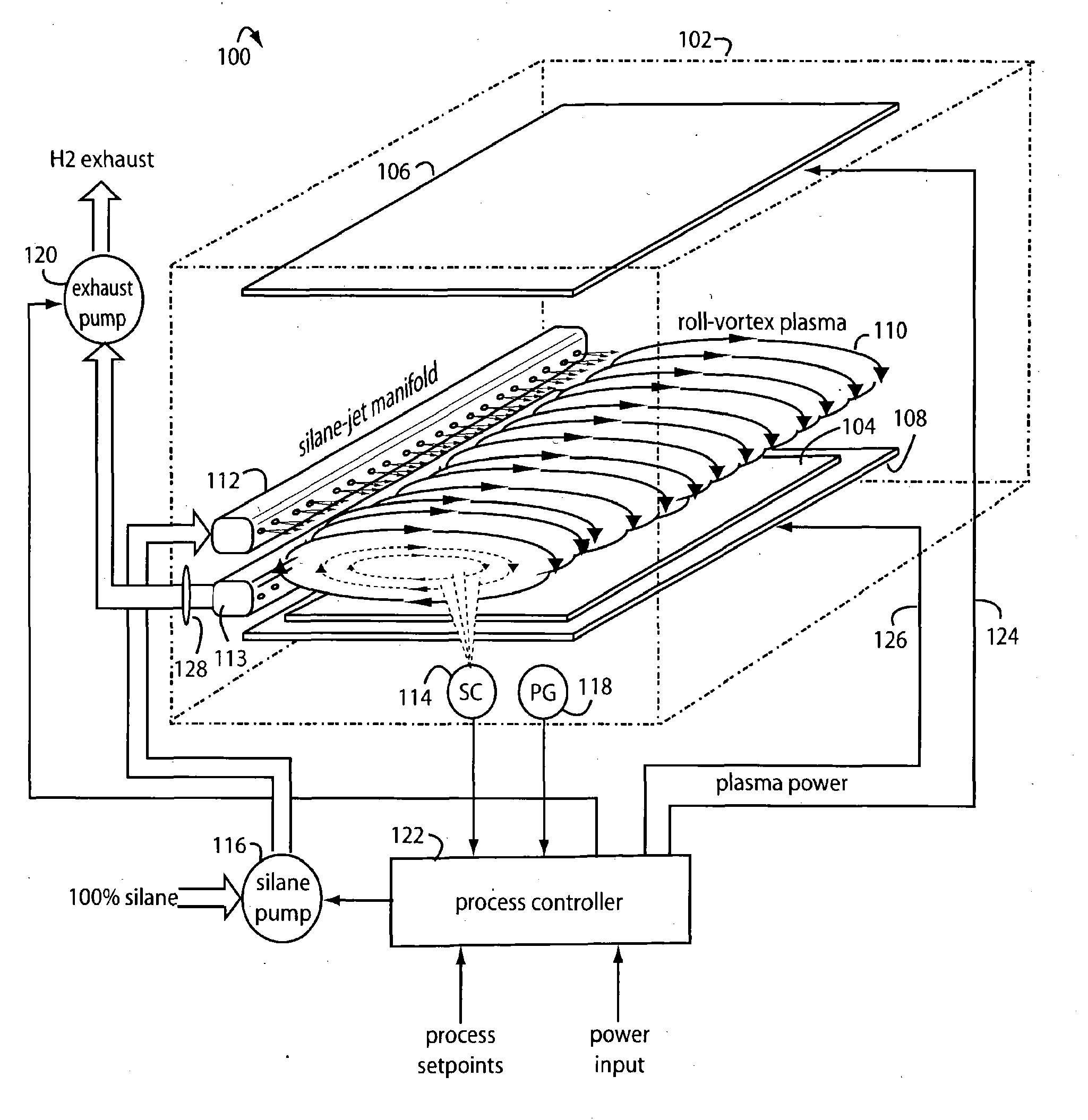
[0029]FIG. 1 illustrates a PECVD system embodiment of the present invention, and is referred to herein by the general reference numeral 100. PECVD system 100 comprises a low-pressure chamber 102 in which a substrate workpiece 104 is transport perpendicular to the axis of roll-vortex plasma 110. A hydrogen atmosphere is introduced into the low-pressure chamber 102. A pair of radio frequency (RF) electrodes 106 and 108 are electrically driven to spawn a plasma 110. Such plasma 110 is rolled into a coaxial vortex by introducing high-velocity silane gas (SiH.sub.4) at near 100% purity just off center from a longitudinal manifold 112. An exhaust manifold 113 assists in rolling the plasma 110 when it draws off excess hydrogen (H.sub.2).

[0030] The silane concentration (SC) in the roll-vortex plasma 110 is maintained at about 6-7% silane-to-hydrogen by observing the relative amplitudes of fluorescence of the constituent gases with a monitor 114. More silane is jetted in by a pump 116 in or...


PUM

PropertyMeasurementUnit
crystalline volume fractionaaaaaaaaaa
Deposition ratesaaaaaaaaaa
pressureaaaaaaaaaa

Abstract

A system comprises a processing chamber for maintaining a hydrogen plasma at low pressure. The processing chamber has a long, wide, thin geometry to favor deposition of thin-film silicon on sheet substrates over the chamber walls. The sheet substrates are moved through between ends. A pair of opposing radio frequency electrodes above and below the workpieces are electrically driven hard to generate a flat, pancaked plasma cloud in the middle spaces of the processing chamber. A collinear series of gas injector jets pointed slightly up on a silane-jet manifold introduce 100% silane gas at high velocity from the side in order to roll the plasma cloud in a coaxial vortex. A second such silane-jet manifold is placed on the opposite side and pointed slightly down to further help roll the plasma and maintain a narrow band of silane concentration. A silane-concentration monitor observes the relative amplitudes of the spectral signatures of the silane and the hydrogen constituents in the roll-vortex plasma and outputs a process control feedback signal that is used to keep the silane in hydrogen concentration at about 6-7%.

Description

RELATED APPLICATION [0001] This is a divisional application of copending U.S. patent application Ser. No. 10 / 618,478, filed Jul. 11, 2003, and to which priority is claimed.FIELD OF THE INVENTION [0002] The present invention relates to semiconductor manufacturing, and more specifically to methods for reducing the costs of fabricating large area thin-film devices like silicon photovoltaic cells. BACKGROUND OF THE INVENTION [0003] Plasma-enhanced chemical vapor deposition (PECVD) can be used to lay down high quality silicon on a variety of substrates. Lower workpiece temperatures can be used when the usual chemical vapor deposition (CVD) is augmented with a hydrogen plasma. Such plasma is typically heated between radio frequency (RF) electrodes, sometimes supplemented with a strong magnetic field to contain the plasma. The RF power, excitation frequency, silane (SiH.sub.4) feed fraction, total gas pressure, gas composition (H.sub.2 only or H.sub.2+Ar) and electrode configuration all ha...

Claims


Application Information

Patent Timeline
Patent Type & Authority Applications(United States)
IPC IPC(8): C23C16/00C23C16/44C23C16/455C23C16/509H01J37/32
CPCC23C16/4412C23C16/45502C23C16/45578H01J37/32449H01J37/32082H01J37/3244C23C16/509
Inventor KESHNER, MARVIN S.JACKSON, WARREN B.NAUKA, KRZYSZTOF
Owner FOREFRONT INNOVATIVE TECH
Why Eureka
Try Eureka