Circuit arrangement for a capacitive proximity switch

a capacitive proximity switch and circuit arrangement technology, applied in the direction of resistance/reactance/impedence, pulse technique, instruments, etc., can solve the problem that the switching process is normally implemented by analog switches, and the cost is relatively high

Inactive Publication Date: 2006-10-26
E G O ELEKTRO GERAETEBAU GMBH
View PDF8 Cites 16 Cited by
  • Summary
  • Abstract
  • Description
  • Claims
  • Application Information

AI Technical Summary

Problems solved by technology

The switching processes are normally implemented by analog switches, which are relatively expensive.

Method used


Image

  • Circuit arrangement for a capacitive proximity switch
  • Circuit arrangement for a capacitive proximity switch
  • Circuit arrangement for a capacitive proximity switch

Examples


Embodiment Construction

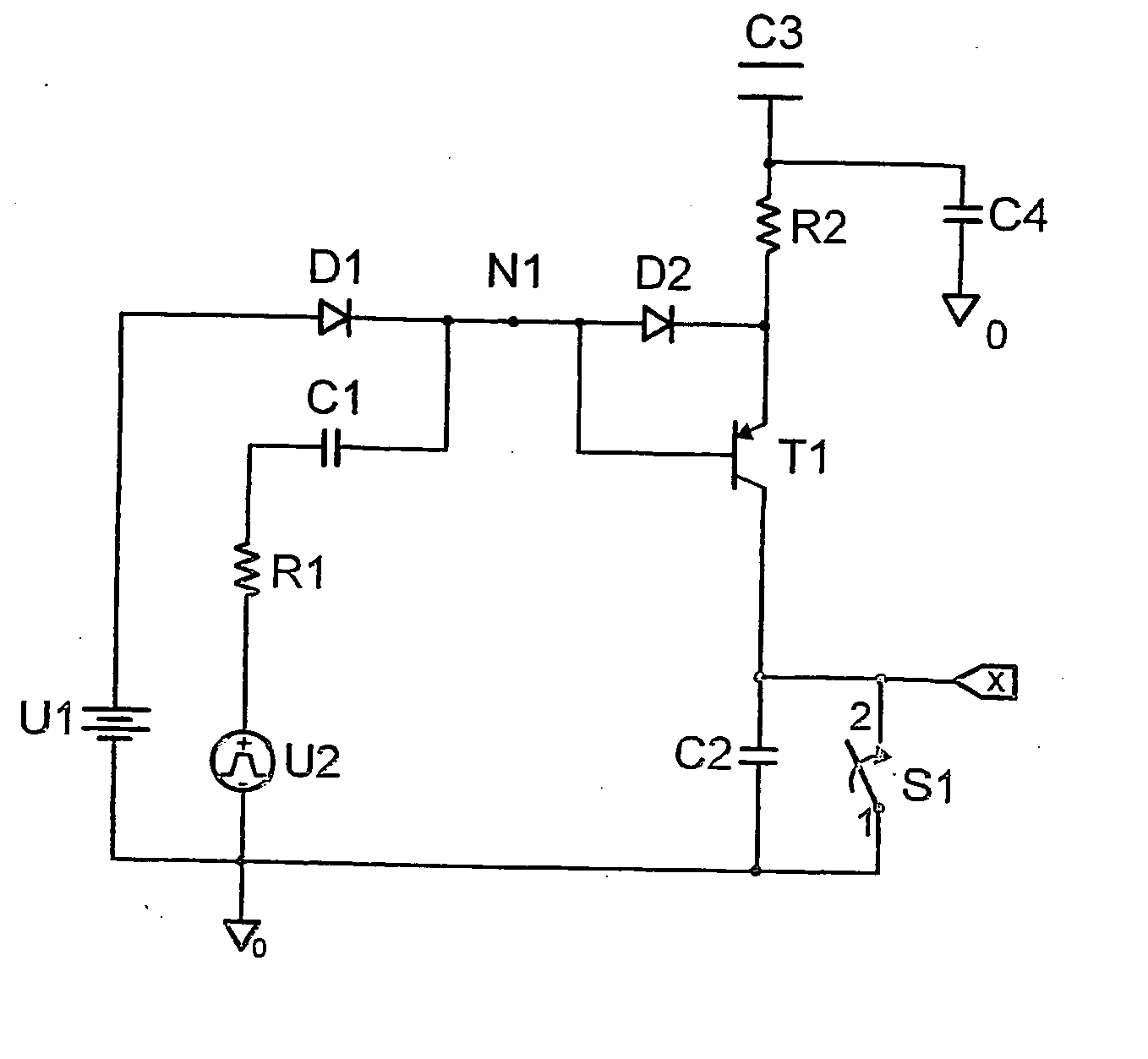
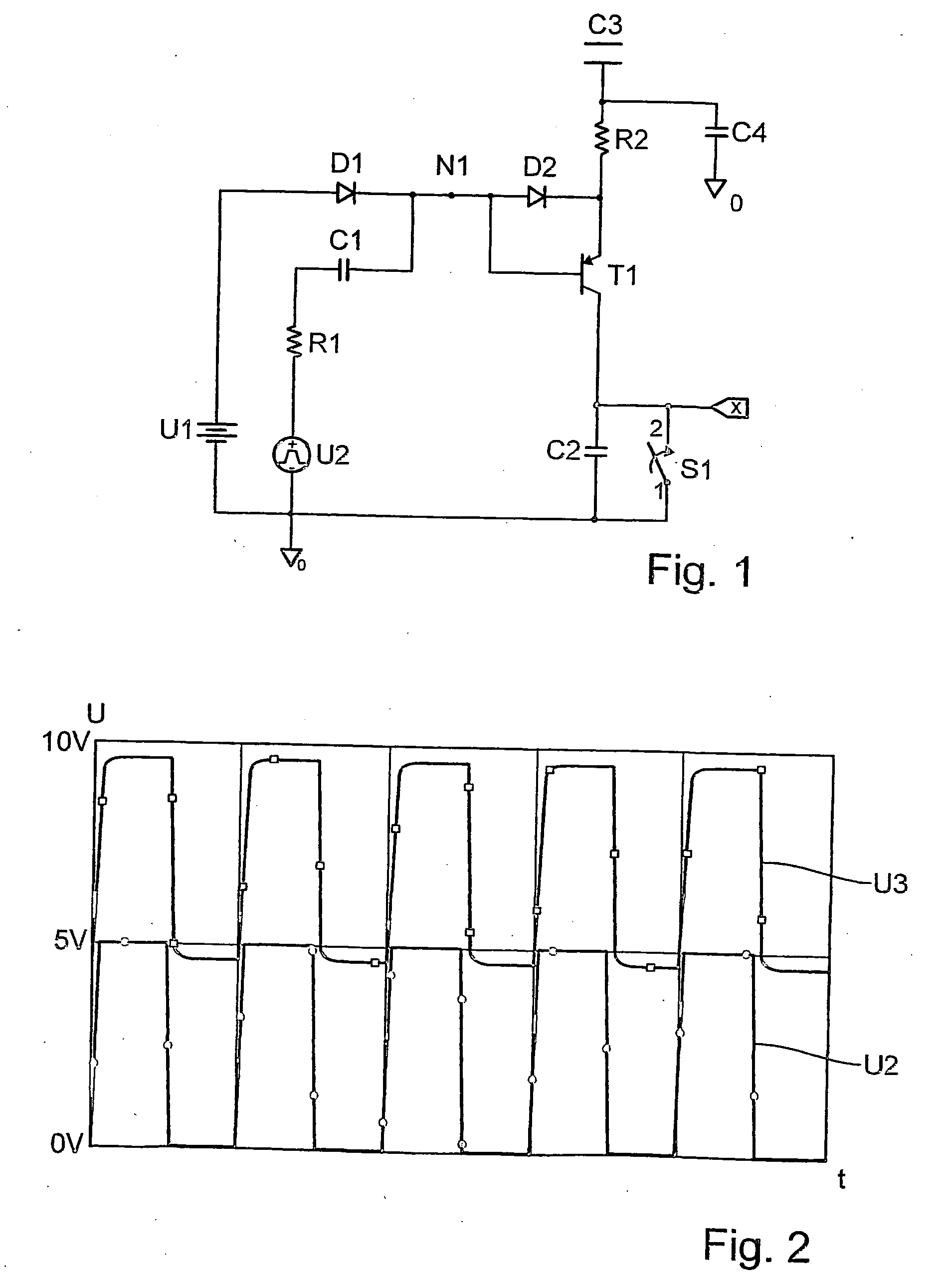
[0020]FIG. 1 is a diagram of a circuit arrangement for capacitive proximity switches for the determination of their operating state. The circuit arrangement comprises a d.c. voltage source U1 and a square-wave voltage source U2 with a common reference potential, e.g. earth, and between the charging voltage node N1 to which a charging voltage is applied and the d.c. voltage source U1 is looped a clamping diode 1 in the non-conducting direction and between the charging voltage node N1 and square-wave voltage source U1 are looped in in series a capacitor C1 and a resistor R1. In conjunction with the capacitor C1, the clamping diode D1 brings about a raising of the voltage at node N1 outputted by the square-wave voltage source U1 by the amount of the voltage of said source. FIG. 2 shows this in a graph of the voltage curve of the a.c. voltage source U2 and the charging voltage U3 at the charging voltage node N1 overtime.

[0021] There is also a first switching means in the form of a diod...


PUM


Abstract

Disclosed is a charge transfer-based circuit arrangement for capacitive proximity switches comprising a capacitive sensor element (C3), the capacity of which changes according to the actuation mode. Said circuit arrangement comprises a central capacitor (C2), a first controllable connecting means (D2) that impinges the capacitive sensor element with a charging voltage (U3) according to a triggering signal, and a second controllable connecting means (T1) which connects the capacitive sensor element to the central capacitor according to the triggering signal in order to transfer the charge from the capacitive sensor element to the central capacitor. The charging voltage can be an AC voltage while the connecting means can be impinged upon by the AC voltage in such a way that the first connecting means or the second connecting means is alternately conductive.

Description

FIELD OF USE AND PRIOR ART [0001] The invention relates to a circuit arrangement for a capacitive proximity switch according to the preamble of claim 1, particularly according to the charge transfer principle. [0002] Circuit arrangements of this type are known and have, e.g. in the case of EP 859 468 A1, a capacitive sensor element, whose capacitance changes as a function of its operating state. This capacitance change is evaluated in order to establish the operating state. For this purpose a charging voltage is supplied to the sensor element, so that as a function of its capacitance and the charging voltage, a specific electric charge is transferred to the sensor element. Following the charging time the sensor element is separated from the charging voltage and connected to a collecting or central capacitor, so that there is a charge transfer from the sensor element to the central capacitor. The charging and subsequent recharging process is repeated for a predetermined number of cyc...

Claims


Application Information

Patent Timeline
Patent Type & Authority Applications(United States)
IPC IPC(8): H03K17/96
CPCH03K2217/960725H03K17/962
Inventor KRAUS, RANDOLF
Owner E G O ELEKTRO GERAETEBAU GMBH
Why Eureka
Try Eureka