Word line driver circuitry and methods for using the same

a driver circuit and word line technology, applied in the field of integrated circuits, can solve the problems of rapid pull down of the word line voltage, and achieve the effects of increasing the refresh rate, rapid pull down of the word line voltage, and high impedance circuitry

Inactive Publication Date: 2006-10-26
MICRON TECH INC
View PDF19 Cites 8 Cited by
  • Summary
  • Abstract
  • Description
  • Claims
  • Application Information

AI Technical Summary

Benefits of technology

[0012] This and other objects of the invention are provided by word line driver circuitry that utilizes a dual transistor arrangement to promote rapid pull down of a word line, while at the same time limiting leakage current when the word line is turned OFF.
[0016] An advantage of this dual transistor arrangement in the word line driver circuitry according to this invention is that the second transistor can be sized to ensure that the word line is pulled down to the deactivation voltage while both transistors are ON. Moreover, the flexibility in sizing the second transistor promotes other advantages such as rapidly pulling down the word line voltage without experiencing substantial bounce on the LOW voltage source. Yet other advantages include increased refresh rates for long rise low transitions and static transitions.
[0017] After the predetermined period of time expires, the second transistor turns OFF, while the first transistor remains ON. Once OFF, the second transistor acts like an “open” switch, thereby preventing current from flowing through the second transistor. An alternative path for current flow is provided by the high impedance circuitry, which couples the first transistor to the LOW voltage source. This high impedance circuitry is effective in limiting leakage current when the word line is deactivated and is also effective in protecting the memory cells from row-to-row shorts and row-to-column shorts.
[0018] When the state of the signal is LOW, the word line driver drives the word line to an activation voltage. The LOW signal causes the first transistor to turn OFF, creating an open “switch” that prevents the low voltage source from pulling the word line down. Once the first transistor is OFF, the word line is pulled HIGH by a high voltage source. Another advantage realized by the dual transistor arrangement is that when the word line is HIGH, leakage current is minimized because the first transistor is OFF.

Problems solved by technology

The time delay, however, ensures that both transistors are either turned ON or OFF, depending on the state (e.g., logic HIGH or LOW) of the signal, for a predetermined period of time.
This results in coupling the word line to a low voltage source via a low impedance pathway that results in rapid pull down of the word line voltage.

Method used


Image

  • Word line driver circuitry and methods for using the same
  • Word line driver circuitry and methods for using the same
  • Word line driver circuitry and methods for using the same

Examples


Embodiment Construction

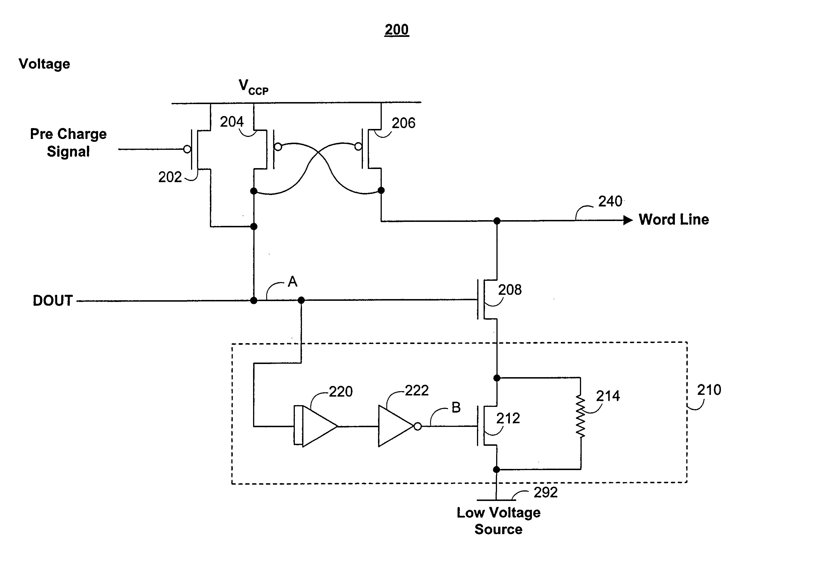
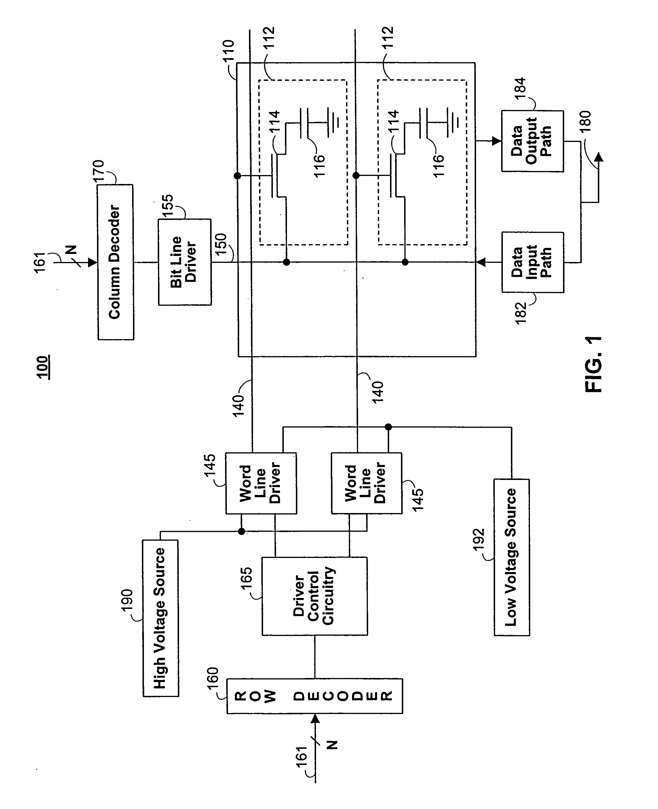
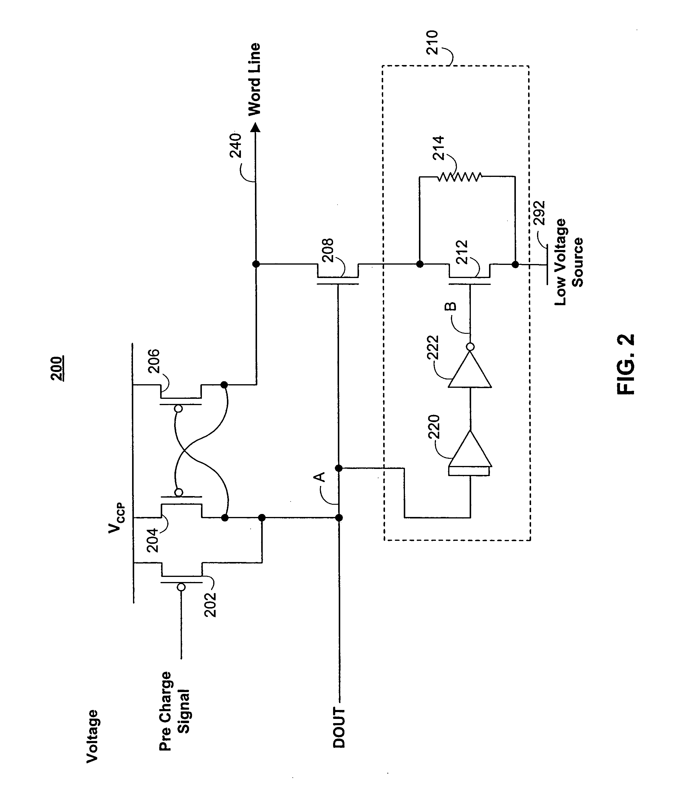
[0028]FIG. 1 shows a memory device 100 having word line driver circuitry 145 according to the invention. FIG. 1 shows that device 100 includes a portion of memory circuitry 110 with two memory cells 112 arranged side-by-side. It is understood that memory circuitry 110 typically includes a plurality of memory cells arranged in rows and columns, but only two such memory cells are shown here for simplicity. Memory circuitry 110 includes word lines 140 and bit lines 150 that are disposed adjacent to the rows and columns of memory cells 112. It is understood that memory circuitry generally includes a plurality of word lines and bit lines, but only two word lines and one bit line are shown here for simplicity. Each memory cell 112 includes a passgate transistor 114 having its gate connected to word line 140, its drain connected to bit line 150, and its source connected to capacitor 116. The layout of the memory cell 112 is typical of that of a DRAM memory cell. Each word line 140 is drive...


PUM


Abstract

Word line driver circuitry for selectively charging and discharging one or more word lines is provided. The driver circuitry uses a dual transistor topology, where a first transistor is driven by a signal, DOUT, and a second transistor is driven by a time-delayed complement of the DOUT, DOUT_BAR. The time delay prevents DOUT_BAR from changing its state immediately after DOUT changes state. As result, both the first and second transistors are turned ON at the same time for a predetermined of time. It is during this time that the voltage on the word line is rapidly driven to a LOW voltage. When the second transistor turns OFF, high impedance circuitry limits the flow of leakage current. This minimizes leakage current when the word line is OFF and when short circuit conditions are present between two or more word lines or between a word line and a bit line.

Description

[0001] This application claims priority from Japanese application No. 2004-245954, filed Aug. 25, 2004, which is incorporated by reference in its entirety. BACKGROUND OF THE INVENTION [0002] The present invention relates to integrated circuitry, and in particular to word line driver circuitry for use in integrated circuitry such as memory. [0003] Memory, such as dynamic random access memory (DRAM) and static random access memory (SRAM), typically include many memory cells that are capable of holding a charge that is representative of a bit of data. Typically, these memory cells are arranged in a two-dimensional array of intersecting rows and columns. Data is written to and retrieved from the memory cells by selectively accessing the memory cells. [0004] Memory cells can be accessed by applying activation voltages to word lines and bit lines. In general, word lines activate memory cells and bit lines provide data to or retrieve data from the activated memory cells. Conventionally, a ...

Claims


Application Information

Patent Timeline
Patent Type & Authority Applications(United States)
IPC IPC(8): G11C8/00
CPCG11C8/08G11C11/413G11C11/4085
Inventor UEDA, HIROKAZU
Owner MICRON TECH INC
Why Eureka
Try Eureka