Method of fabricating a one transistor floating-body DRAM cell in bulk CMOS process with electrically isolated charge storage region

Inactive Publication Date: 2005-07-05
MOSYS INC
View PDF11 Cites 284 Cited by
  • Summary
  • Abstract
  • Description
  • Claims
  • Application Information

AI Technical Summary

Benefits of technology

[0014]In accordance with the present invention, a buried region of the first conductivity type is located under the source region, drain region and floating body region. The buried region helps to form

Problems solved by technology

Moreover, significant area is required to form the capacitor needed for storage of signal charge.
One significant disadvantage of conventional 1T/FB DRAM cell 100 is that it requires the use of partially depleted silicon-on-insulator (PD-SOI) process, which is relatively expensive and not widely available.
In addition, the floating body effect of the SOI process, although utilized in the 1T/FB DRAM cell advanta

Method used


Image

  • Method of fabricating a one transistor floating-body DRAM cell in bulk CMOS process with electrically isolated charge storage region
  • Method of fabricating a one transistor floating-body DRAM cell in bulk CMOS process with electrically isolated charge storage region
  • Method of fabricating a one transistor floating-body DRAM cell in bulk CMOS process with electrically isolated charge storage region

Examples


Embodiment Construction

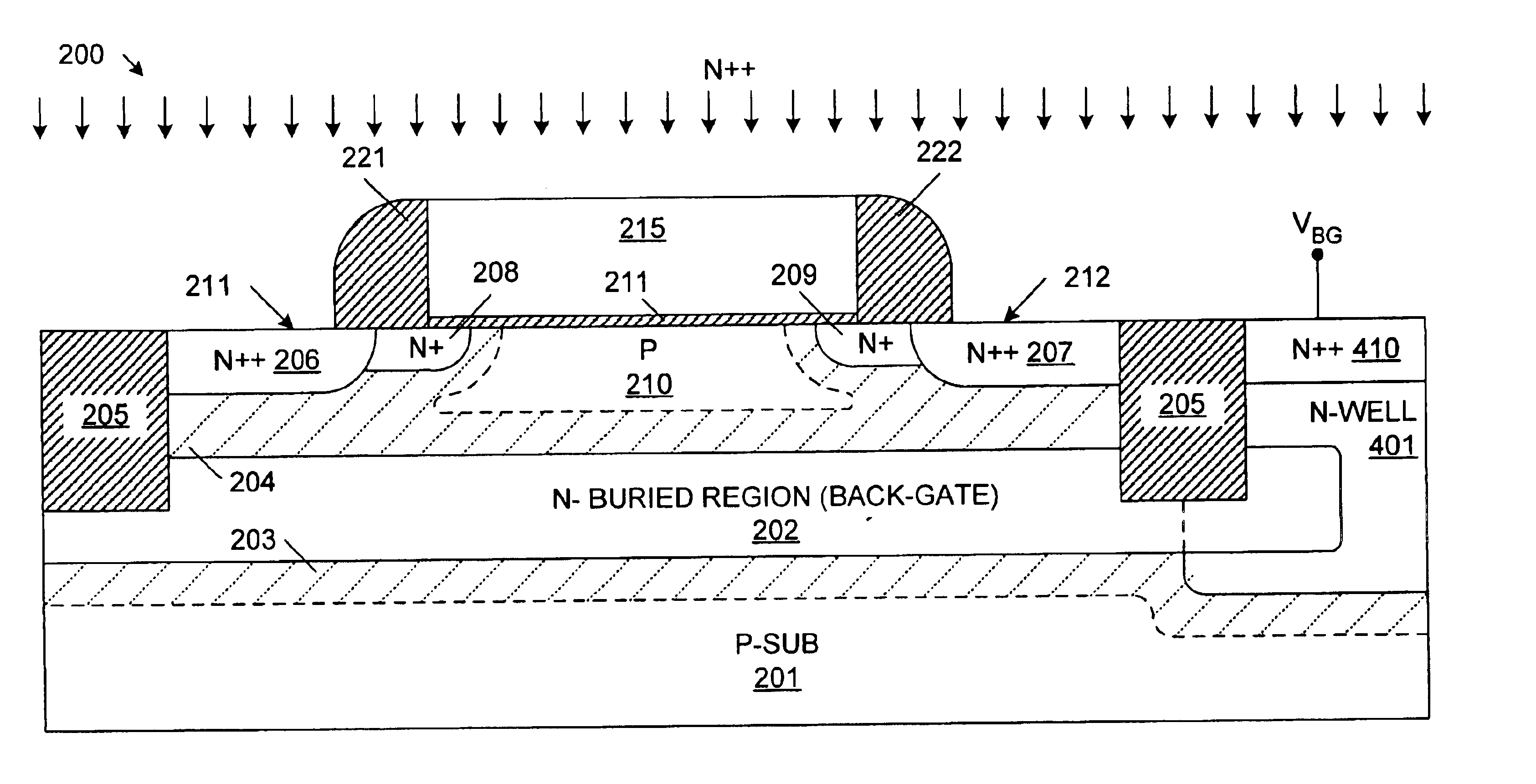
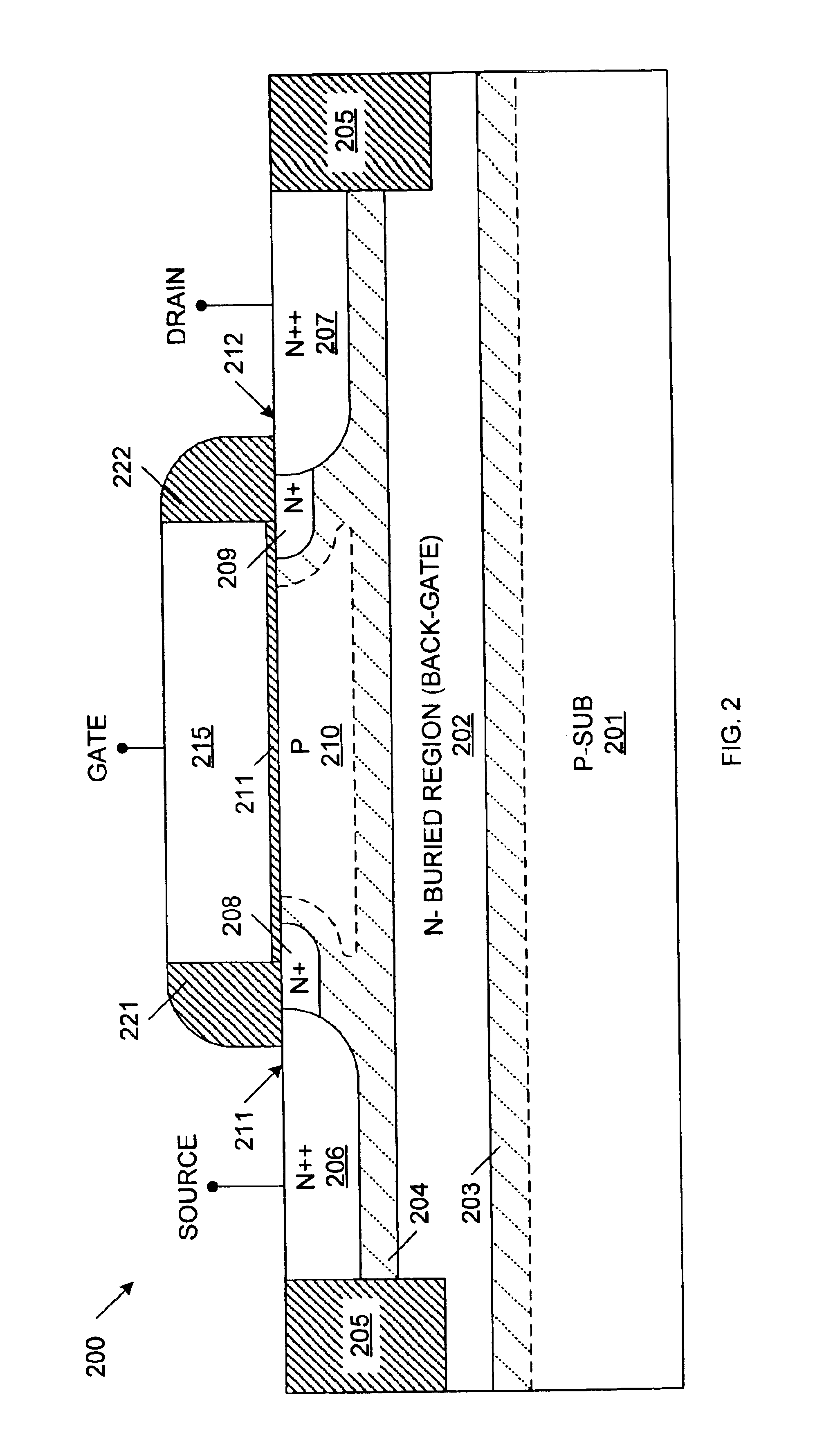
[0032]FIG. 2 is a cross-sectional view of an NMOS 1T / FB DRAM cell 200 in accordance with one embodiment of the present invention. Although the present embodiment describes a 1T / FB DRAM cell that uses an NMOS transistor, it is understood that either NMOS or PMOS transistors can be used to form 1T / FB DRAM cells in accordance with the present invention. When a PMOS transistor is used to implement the 1T / FB DRAM cell, the conductivity types of the various elements are reversed.

[0033]DRAM cell 200 includes P− type silicon substrate 201, N− type buried region (or back-gate) 202, depletion regions 203-204, shallow trench isolation (STI) regions 205, heavily-doped N++ type source and drain regions 206 and 207, lightly-doped N+ type source and drain regions 208 and 209, P type floating body region 210, gate oxide layer 211, gate electrode 215 and sidewall spacers 221-222.

[0034]N++ type source region and N+ type source region combine to form n-type source region 211. Similarly, N++ type drain...


PUM


Abstract

A one-transistor, floating-body (1T/FB) dynamic random access memory (DRAM) cell is provided that includes a field-effect transistor fabricated using a process compatible with a standard CMOS process. The field-effect transistor includes a source region and a drain region of a first conductivity type and a floating body region of a second conductivity type, opposite the first conductivity type, located between the source region and the drain region. A buried region of the first conductivity type is located under the source region, drain region and floating body region. The buried region helps to form a depletion region, which is located between the buried region and the source region, the drain region and the floating body region. The floating body region is thereby isolated by the depletion region. A bias voltage can be applied to the buried region, thereby controlling leakage currents in the 1T/FB DRAM cell.

Description

RELATED APPLICATIONS[0001]The present invention is a divisional of U.S. patent application Ser. No. 10 / 095,901 filed Mar. 11, 2002, now U.S. Pat. No. 6,661,042, and is related to commonly owned, co-filed U.S. patent application Ser. No. 10 / 095,984 filed Mar. 11, 2002, now U.S. Pat. No. 6,686,624.BACKGROUND OF THE INVENTION[0002]1. Field of the Invention[0003]The present invention relates to a dynamic random access memory (DRAM) cell, as well as methods for operating and fabricating a DRAM cell. More specifically, the present invention relates to a one-transistor floating-body DRAM cell formed using a process compatible with a bulk CMOS process, wherein charge is stored inside an electrically isolated body region underneath the transistor channel region.[0004]2. Related Art[0005]conventional one-transistor, one-capacitor (1T / 1C) DRAM cells require a complex process for fabrication. Moreover, significant area is required to form the capacitor needed for storage of signal charge. Recen...

Claims


Application Information

Patent Timeline
IPC IPC(8): H01L27/148H01L21/70H01L21/8242H01L29/768H01L29/66H01L27/02H01L27/108
CPCH01L27/108H01L27/10802H01L29/7841H01L27/0214H01L27/10873H10B12/20H10B12/00H10B12/05
Inventor HSU, FU-CHIEH
Owner MOSYS INC
Why Eureka
Try Eureka