
Laser diode structure with blocking layer

a diode and laser technology, applied in semiconductor lasers, laser details, electrical equipment, etc., can solve the problems of reducing the efficiency of the threshold current and slope, reducing the performance and reliability of the device, and reducing the efficiency of the laser. the effect of reducing the cost and time of production and easing the manufacturing method

Inactive Publication Date: 2005-06-30
NORTEL NETWORKS UK +1
View PDF12 Cites 5 Cited by
  • Summary
  • Abstract
  • Description
  • Claims
  • Application Information

AI Technical Summary

Benefits of technology

[0017] It is an object of the present invention to provide a semiconductor laser fabricated on a p-substrate having improved lateral current performance compared to the ridge waveguide laser, and a simpler fabrication process than a laser with a buried heterostructure.
[0020] The manufacturing method can be eased by the use of iron-doped indium phosphide and may reduce the cost and time to produce the self-aligned laser structure when compared to a buried heterostructure.

Problems solved by technology

This structure, however, suffers from excessive lateral leakage current due to the high electron mobility in InP based materials, significantly degrading the threshold current and the slope efficiency, and rendering the lasers inefficient and less attractive for real applications.
These processes may introduce nonradiative recombination centres close to the active region, degrading performance and the reliability of the device.
Also, high doping levels close to the area of high optical intensity can increase the optical losses, making such devices less attractive for high power applications.
Moreover, in a buried heterostructure, it is difficult to optimise the growth of the blocking layers to minimise potential leakage current-paths.
The growth of the active region, however which is a critical part of the laser, happens in an overgrowth step, which might raise questions about its quality.
Ridge-waveguide lasers on p-doped substrate suffer from excessive lateral current leakage because of the high electron mobility in InP based material.
This excessive lateral leakage current can degrade the threshold current and the slope efficiency rendering the lasers inefficient and less attractive for real applications.
However, one potential problem with this structure on p-substrate is the lateral leakage that can occur below the p-blocking layer.
Current that progresses sideways is essentially lost thereby decreasing the overall efficiency of the laser.
One option would be to remove layer 41, however this would result in the elimination of a reverse bias pn-junction and as such the current would not be confined to the trench, consequently resulting in a poor performing laser.
Design changes have been introduced aimed at meeting these requirements, however a problem relating to lateral current leakage remains, together with its other potential associated inefficiencies.
This leakage current can be caused by a lack of containment at the edges of the active region, thereby allowing current to flow away from the area of interest.
Techniques have been proposed to solve this problem, but have been unable to meet the requirements of ease of fabrication and the control of the leakage current.
Buried heterostructures solve some aspects of the leakage current problem, but require multiple process steps and can produce nonradiative recombination centres which can degrade performance.
Channel guide lasers on p-substrate can use an overgrowth on the active region, which being a critical part of the laser can cause quality problems and limit optimisation of a design.
The use of a p-blocking layer is limited by the lateral leakage that can occur below this layer.

Method used


Image

  • Laser diode structure with blocking layer
  • Laser diode structure with blocking layer
  • Laser diode structure with blocking layer

Examples


Embodiment Construction

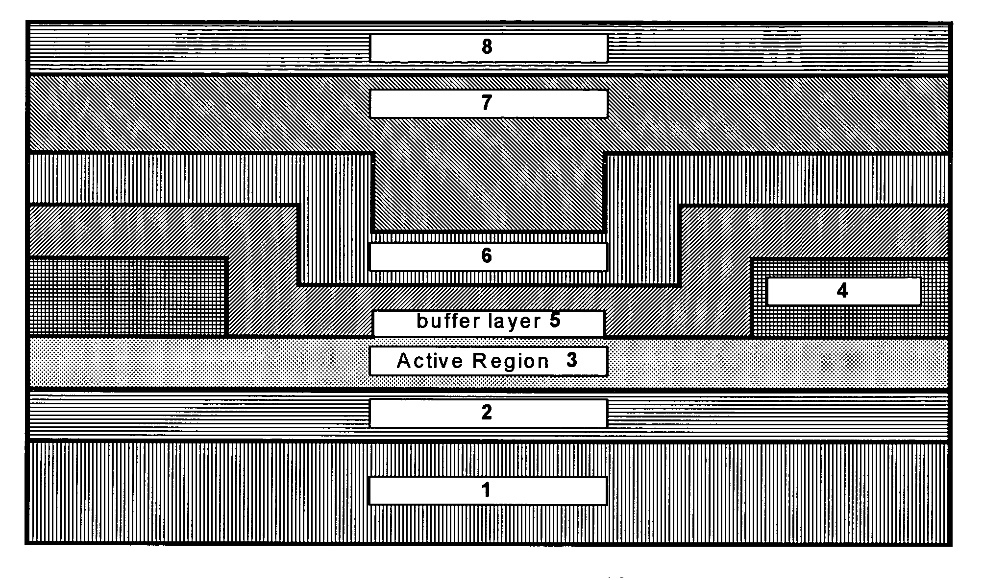
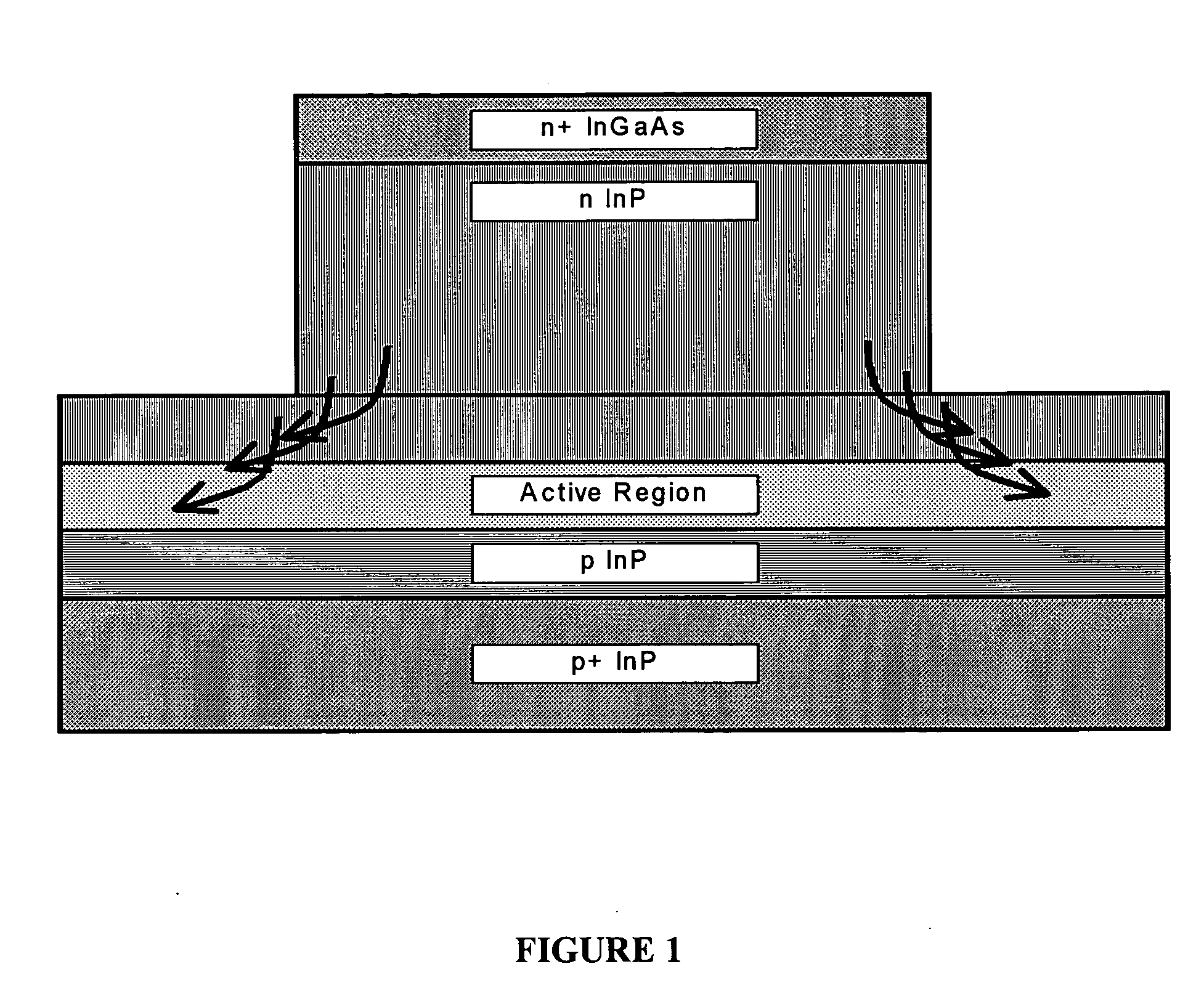
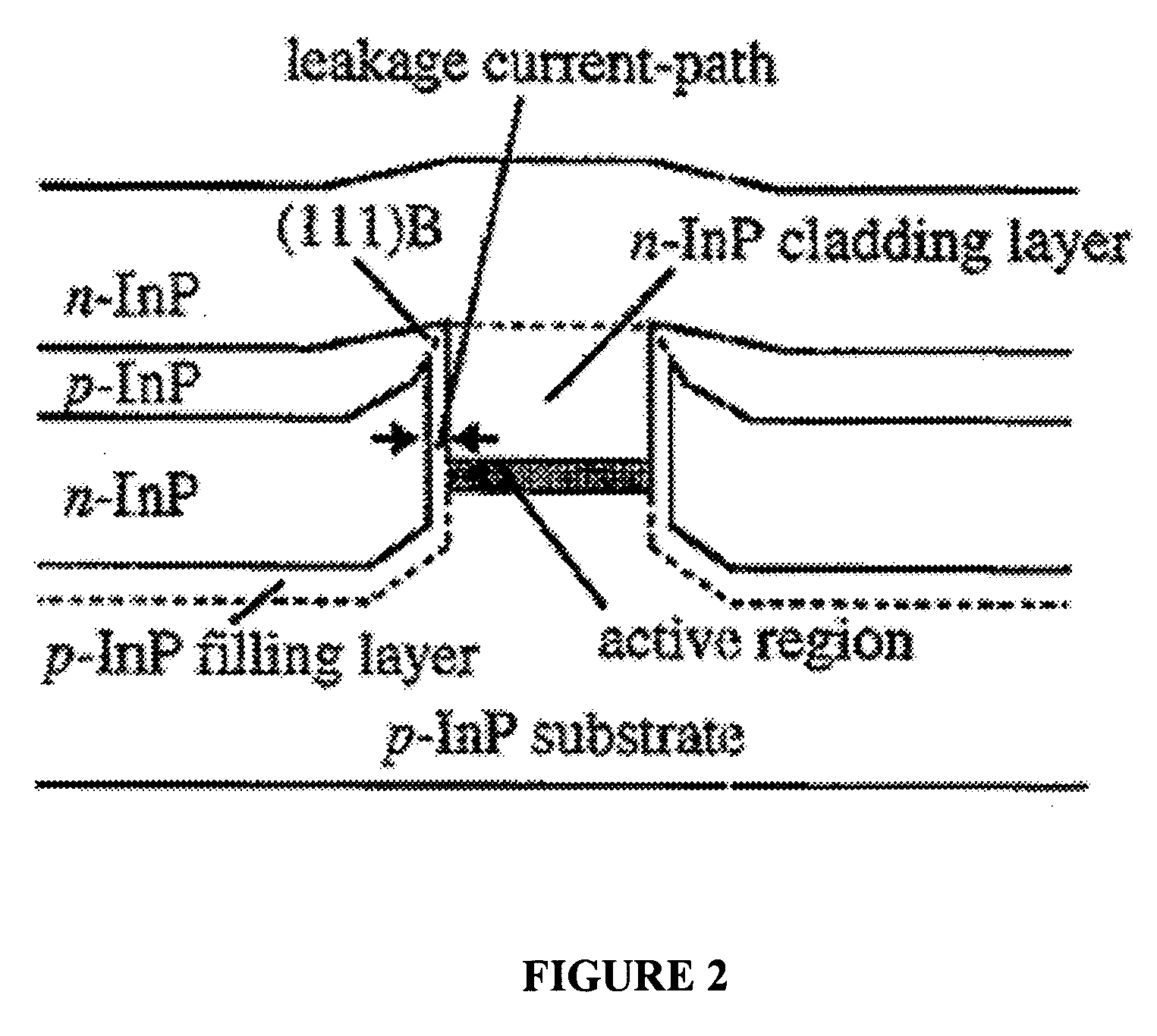
[0031] The present invention provides a self-aligned laser structure that can be fabricated on a p-substrate and provides a means for limiting the leakage current thereby improving the overall efficiency of the structure. The waveguide laser structure comprises a first series of layers deposited in sequence upon a p-InP, p-GaAs or p-GaN substrate or other form of p-substrate, wherein these layers form the p-clad layer. An active layer is subsequently deposited upon this first series of layers. A blocking layer of insulating or semi-insulating material is deposited upon the active layer, wherein this blocking layer has a trench formed therein, wherein this semi-insulating layer or layers are epitaxially deposited. A semi insulating material forming the blocking layer is defined as a material that inhibits electron or hole currents by trapping carriers. The blocking layer provides a means for limiting current flow therethrough, thereby reducing leakage current. Upon the blocking layer...


PUM


Abstract

The present invention provides a self-aligned laser structure that can be fabricated on a p-substrate and provides a means for limiting the leakage current thereby improving the overall efficiency of the structure. The waveguide laser structure comprises a first series of layers deposited in sequence upon a p-InP, p-GaAs or p-GaN substrate or other form of p-substrate, wherein these layers form the p-clad layer. An active layer is subsequently deposited upon this first series of layers. A blocking layer of insulating or semi-insulating material is deposited upon the active layer, wherein this blocking layer has a trench formed therein, wherein this semi-insulating layer or layers are epitaxially deposited. The blocking layer provides a means for limiting current flow therethrough, thereby reducing leakage current. Upon the blocking layer are deposited a second series of layers completing the laser structure, wherein this second series of layers form the n-clad layer. Since the n-clad layer contains more than one material, the structure provides lateral waveguiding. Upon the completion of the deposition of all of the layers, a positive electrode is formed on the bottom surface of the first series of layers and a negative electrode is formed on the top of the second series of layers.

Description

[0001] This application claims the benefit of U.S. Patent Application Ser. No. 60 / 479,868 filed Jun. 20, 2003.FIELD OF THE INVENTION [0002] The present invention pertains to the field of semiconductor lasers and more particularly to semiconductor lasers fabricated using p-substrate. BACKGROUND [0003] The ridge waveguide laser is a semiconductor light-emitting device that includes a ridge-shaped layer on a semiconductor wafer. It is one of the simplest and most reliable laser devices available today. One such laser and its fabrication process has been described in an article “High Power Ridge-Waveguide AlGaAs GRINSCH Laser Diode” by C. Harder et al. (published in Electronics Letters, Sep. 25, 1986, Vol. 22, No. 20, pp. 1081-1082). [0004] In the past, most of the efforts made in designing semiconductor lasers were directed to GaAs system devices operating at a wavelength of about 0.8 μm. However more recently and particularly for communication applications, lasers emitting beams of a ...

Claims


Application Information

Patent Timeline
IPC IPC(8): H01S5/00H01S5/22H01S5/223H01S5/323
CPCH01S5/2224H01S5/2231H01S5/32391H01S5/2237H01S5/2232
Inventor REID, BENOITFILY, ARNAUD CHRISTIANLICHTENSTEIN, NORBERTKNIGHT, D. GORDON
Owner NORTEL NETWORKS UK
Learn More