Semiconductor laser device

a semiconductor laser and laser technology, applied in semiconductor lasers, instruments, record information storage, etc., can solve problems such as difficulties in multi-wavelength semiconductor laser devices

Inactive Publication Date: 2006-10-26
PANASONIC CORP
View PDF4 Cites 25 Cited by
  • Summary
  • Abstract
  • Description
  • Claims
  • Application Information

AI Technical Summary

Benefits of technology

[0020] In the second semiconductor laser device, the first dielectric film and the second dielectric film of the present invention are formed at the reflection facets located opposite the light emitting facets for emitting the respective laser lights of the first semiconductor laser element and the second semiconductor laser element, and the third diel...

Problems solved by technology

Under the circumstances, it is difficult for the multi-wavelength semiconductor laser devices disclosed in References 1 and 2 to attain high power output operation necessary for writing into various recording media such as DVD-RAM, DVD-R, CD-R, and the like.
Also, Reference 3 merely refers to a general technique f...

Method used


Image

  • Semiconductor laser device
  • Semiconductor laser device
  • Semiconductor laser device

Examples


Embodiment Construction

[0037] One embodiment of the present invention will be described in detail with reference to accompanying drawings.

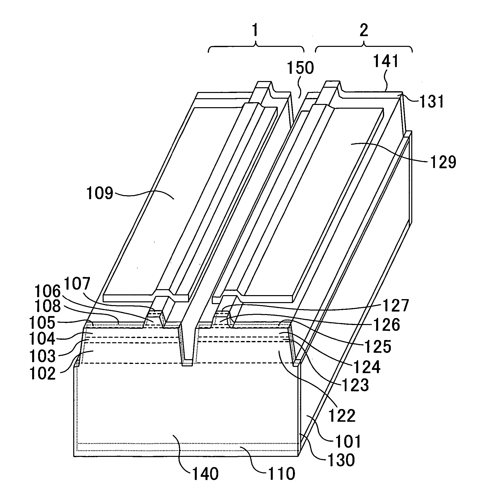
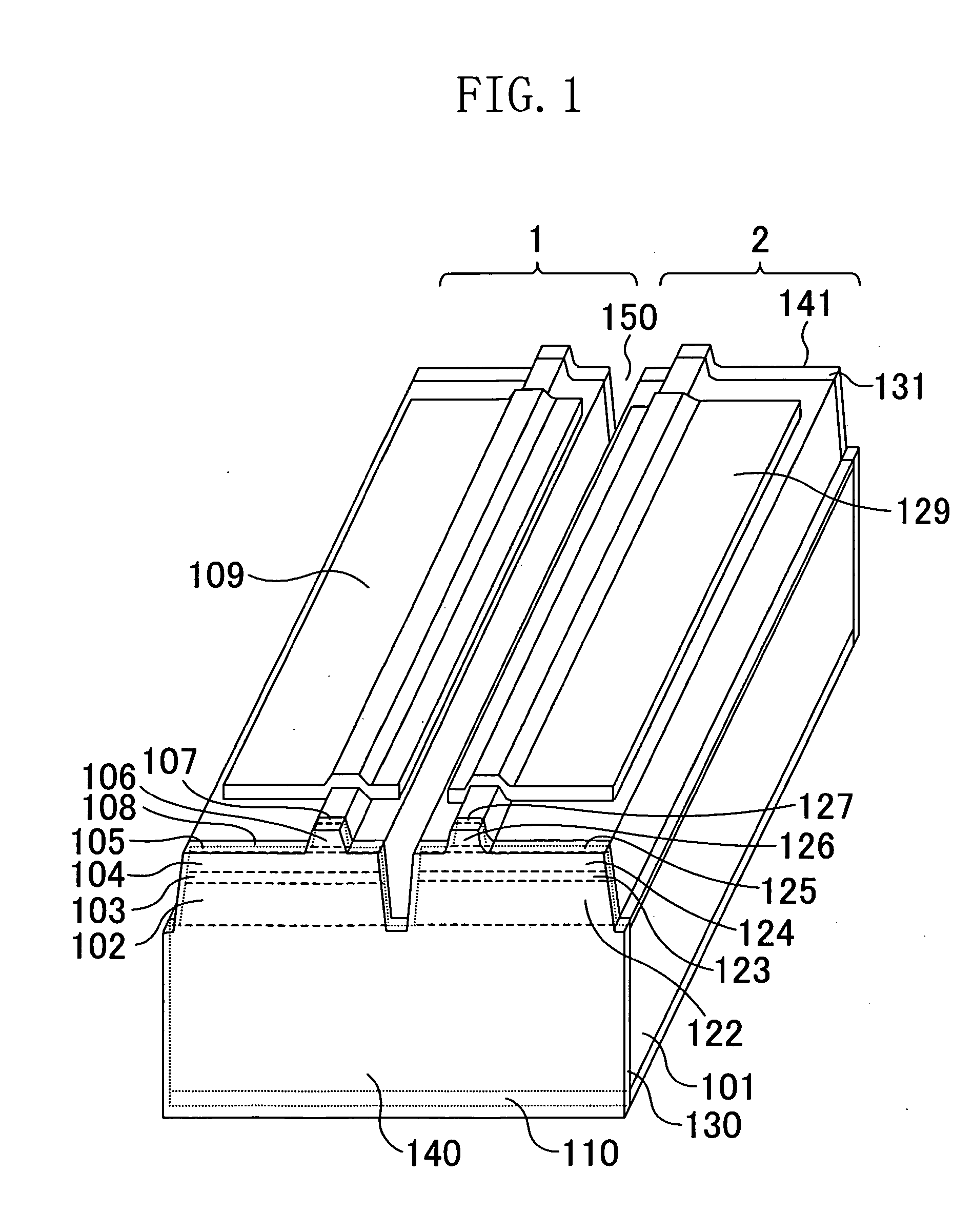
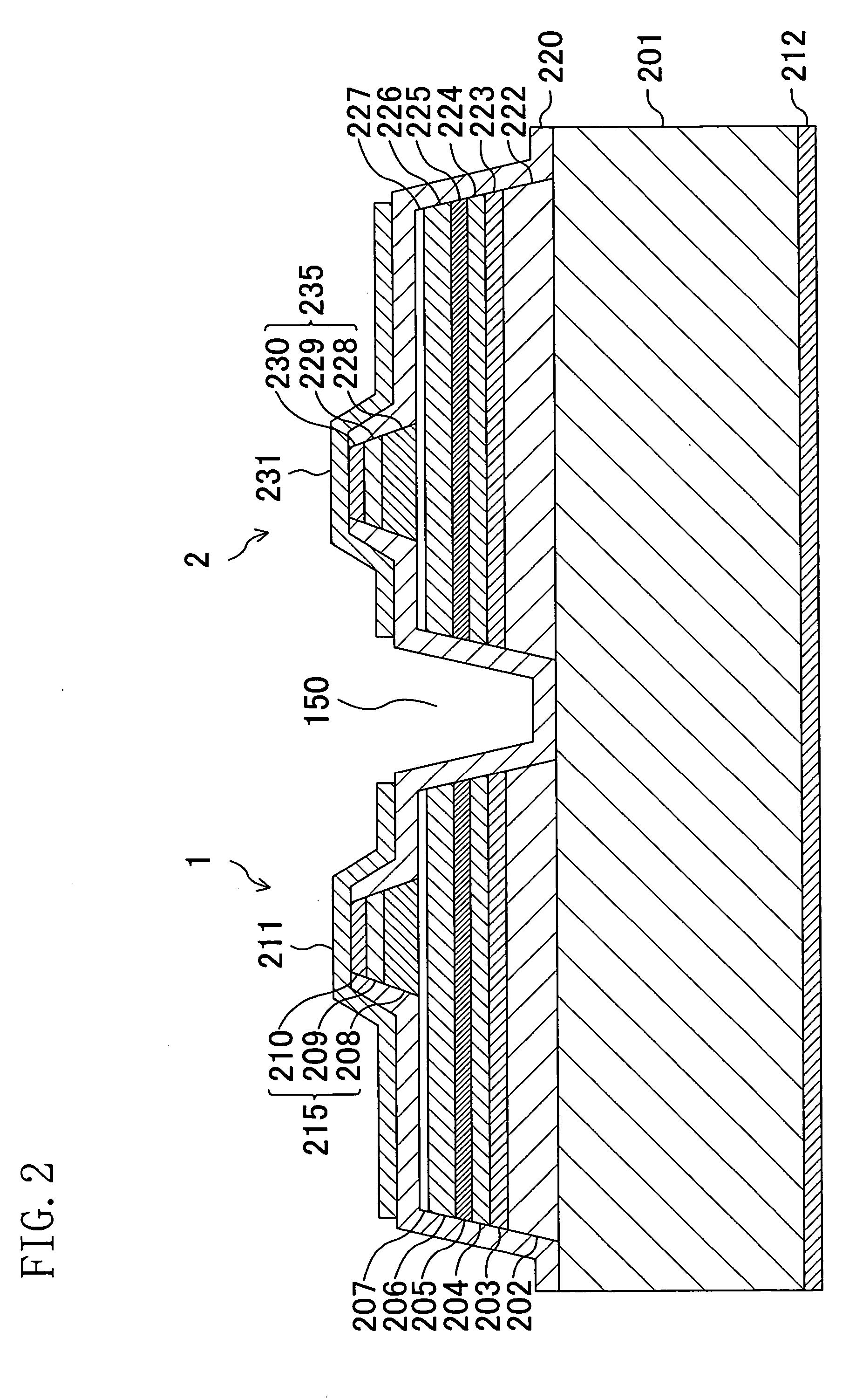
[0038]FIG. 1 shows the schematic structure of a dual-wavelength semiconductor laser device according to one embodiment of the present invention. As shown in FIG. 1, in the dual-wavelength semiconductor laser device according to the present embodiment, a red semiconductor laser element 1 for generating a laser light having a band at 660 nm and an infrared semiconductor laser element 2 for generating a laser light having a band at 780 nm are formed on a substrate 101 monolithically.

[0039] The red semiconductor laser element 1 is so structured that a first n-type cladding layer 102, a first active layer 103, a first p-type cladding layer 104, a first etch stop layer 105, a second p-type cladding layer 106, a first p-type contact layer 107, and an insulating layer 108 are formed sequentially in this order on the substrate 101 for epitaxial growth.

[0040] The infrared semi...


PUM


Abstract

A semiconductor laser device includes a first semiconductor laser element for emitting a first laser light having a first oscillation wavelength of λ1 and a second semiconductor laser element for emitting a second laser light having a second oscillation wavelength of λ2 (wherein λ2≧λ1), which are formed on a single substrate. A first dielectric film which has a refractive index of n1 with respect to a wavelength λ between the first oscillation wavelength λ1 and the second oscillation wavelength λ2 and has a film thickness of approximately λ/(8n1) is formed at light emitting facets in the first semiconductor laser element and the second semiconductor laser element, from which the laser lights are emitted, and a second dielectric film having a refractive index of n2 and a film thickness of λ/(8n2) are formed on the first dielectric film.

Description

CROSS REFERENCE TO RELATED APPLICATIONS [0001] This Non-provisional application claims priority under 35 U.S.C. § 119(a) on Patent Application No. 2005-128740 filed in Japan on Apr. 26, 2005, the entire contents of which are hereby incorporated by reference. BACKGROUND ART [0002] The present invention relates to a single-wavelength or dual-wavelength semiconductor laser device used as a light source for an optical disk. [0003] Semiconductor laser devices are widely employed in various fields such as electronics, optoelectronics, and the like, and are indispensable to optical devices. Especially, optical disks such as CDs (compact disks), DVDs (digital versatile disks), and the like are utilized increasingly as large-capacity recording media. The recording media used in the DVDs are smaller in pit length and track interval than the recording media used in the CDs. Accordingly, the wavelength of the laser light used in the DVDs is shorter than that used in the CDs. Specifically, the o...

Claims


Application Information

Patent Timeline
IPC IPC(8): H01S5/00
CPCB82Y20/00G11B7/1275G11B2007/0006H01S5/028H01S5/0287H01S5/162H01S5/4087H01S5/2231H01S5/34313H01S5/34326H01S5/3436H01S5/4031H01S5/2214
Inventor KUME, MASAHIROSHIMAMOTO, TOSHITAKAKIDOGUCHI, ISAOUNO, TOMOAKI
Owner PANASONIC CORP
Why Eureka
Try Eureka