Image pickup device and method of manufacturing the same

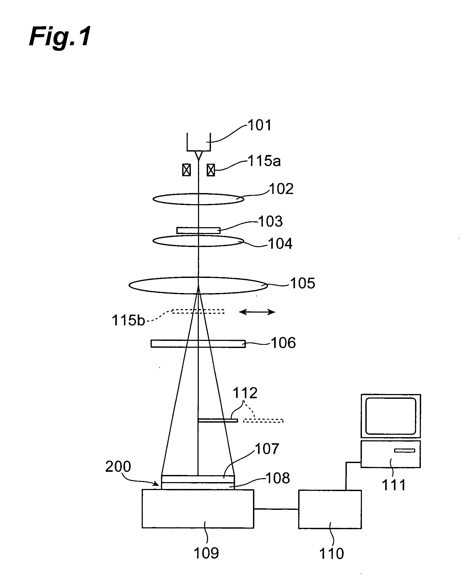
a pickup device and image technology, applied in the direction of radiation intensity measurement, television system, radio control device, etc., can solve the problem that the yield of the process of joining fop b>108/b> and semiconductor substrate b>109/b> cannot be improved above a certain level, and achieve the effect of facilitating positioning in the process of joining fop to the semiconductor substra

Active Publication Date: 2006-10-26
HAMAMATSU PHOTONICS KK
View PDF1 Cites 25 Cited by
  • Summary
  • Abstract
  • Description
  • Claims
  • Application Information

AI Technical Summary

Benefits of technology

[0009] In the image pickup device according to the present invention, since the FOP and the CCD reading part do not contact each other directly as described above, excess current from the FOP will not flow directly to the CCD reading part during the joining of the FOP to the semiconductor substrate and electrostatic discharge of the CCD reading part is thus restrained effectively.
[0011] The semiconductor substrate has a structure such that a recess is formed at a portion of the back surface corresponding to the region at which the CCD reading part is disposed and the thickness of the region at which the CCD reading part is disposed is thinner than the remaining region. By a part of the FOP being fitted in this thin part, the back surface of the semiconductor substrate and the light outgoing end surface of the FOP are joined. By this arrangement, the thickness of the semiconductor substrate, through which the light emitted from the FOP is transmitted until it is detected by the CCD reading part, is made thin and light of shorter wavelength can be detected at high sensitivity. Also, by forming the thin part, positioning in the process of joining the FOP to the semiconductor substrate is facilitated.
[0012] To the front surface of the semiconductor substrate, a protective plate is preferably joined so as to cover the entirety of the CCD reading part. By this arrangement, the CCD reading part is protected from contamination, etc., and the semiconductor substrate is reinforced mechanically.
[0015] As described above, in the image pickup device according to the present invention, since the light outgoing end surface of the FOP and the CCD reading part do not contact each other directly and an excess current therefore does not flow to the CCD reading part in the process of joining the FOP to the semiconductor substrate, electrostatic discharge of the CCD reading part is restrained effectively.
[0019] As described above, since a part of the FOP is fitted into the thin part (recess) formed in the back surface of the semiconductor substrate, the distance between the light outgoing end surface of the FOP and the CCD reading part is shortened and light of shorter wavelength can be detected at high sensitivity. Also, by the forming of the thin part in the back surface of the semiconductor substrate, positioning in the process of joining the FOP to the semiconductor substrate is facilitated. Also, a guiding opening is provided in the guide member that is mounted to the other opening portion of the package, and this guiding opening functions as a reference member in the process of inserting at least a part of the FOP inside the cavity and facilitates positioning in the process of joining the FOP to the semiconductor substrate.
[0023] Thus, in the image pickup device manufacturing method according to the present invention, the CCD reading part and the light outgoing end surface of the FOP do not contact each other directly in the step of joining the FOP and the semiconductor substrate, thereby preventing the flowing of excess current from the FOP to the CCD reading part. Electrostatic discharge of the CCD reading part is thus restrained and the manufacturing yield of the image pickup device is thus improved.

Problems solved by technology

However, the yield of the process of joining FOP 108 and semiconductor substrate 109 could not be improved above a certain level.

Method used


Image

  • Image pickup device and method of manufacturing the same
  • Image pickup device and method of manufacturing the same
  • Image pickup device and method of manufacturing the same

Examples


first embodiment

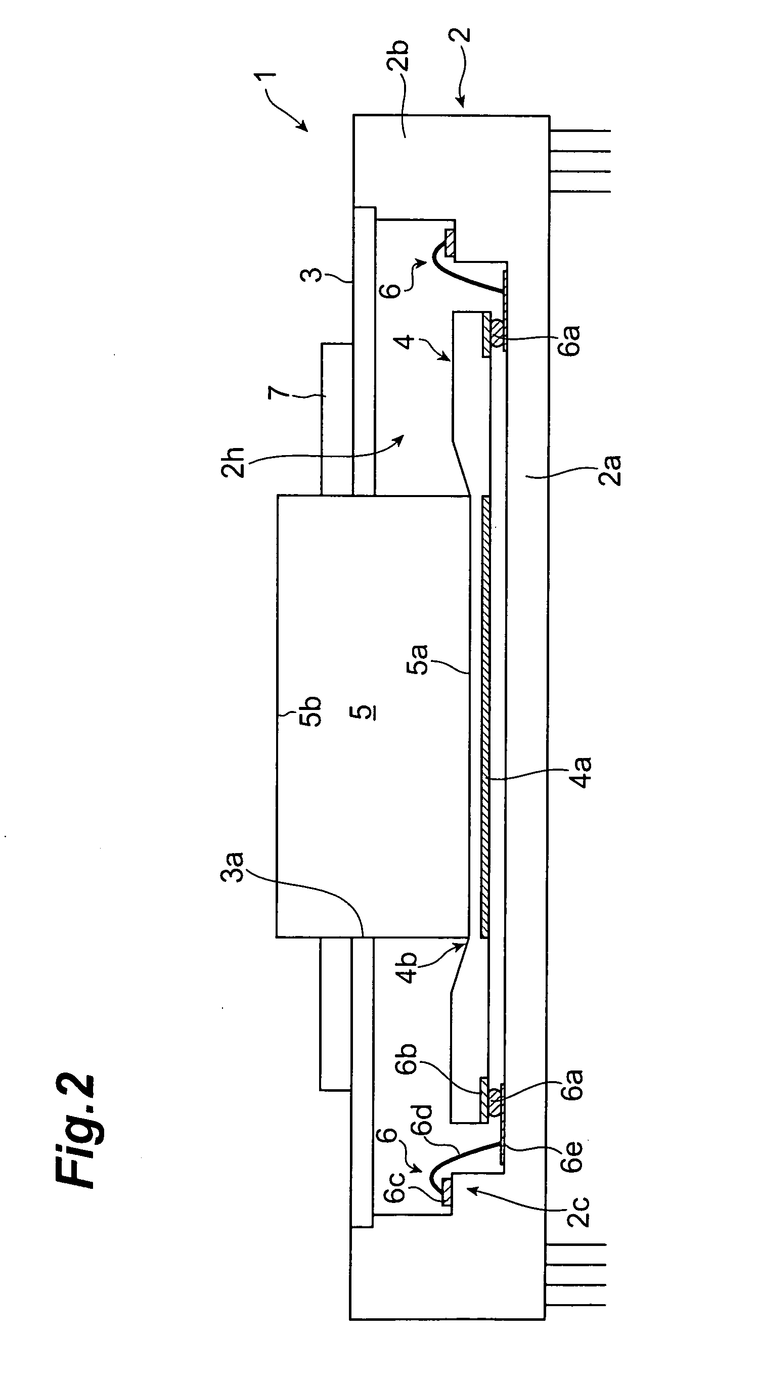
[0039]FIG. 2 is a diagram showing the cross-sectional structure of a first embodiment of an image pickup device according to the present invention. In image pickup device 1 of this first embodiment, a semiconductor substrate 4, having a CCD reading part 4a, is housed inside a cavity 2h of a package 2, and the semiconductor substrate 4 is optically coupled to an FOP 5.

[0040] The image pickup device 1 comprises a package 2, having the cavity 2h surrounded by a bottom surface part 2a and the side wall parts 2b, a cover 3 covering an opening of package 2, the semiconductor substrate 4 comprised of silicon, etc. and having CCD reading part 4a formed on a front surface side, FOP 5 joined to the semiconductor substrate 4, and electrical wirings 6 for taking out charge signals output from the CCD reading part 4a to the exterior of the package 2.

[0041] The cover 3 is formed with a guiding opening 3a for insertion of at least a part of the FOP 5 into the cavity 2h.

[0042] The semiconductor ...

second embodiment

[0062] The arrangement of a second embodiment of an image pickup device according to the present invention shall now be described using FIG. 5. Though the image pickup device 20 of this second embodiment has substantially the same structure as the above-described first embodiment, it differs in that a Peltier element 8, for cooling a CCD reading part 4a, is housed inside a cavity 2h of a package 2, a protective plate 9 is adhered onto a front surface (surface on which the CCD reading part 4a is formed) of a semiconductor substrate 4, a guide member 12 serves in common as the first embodiment's cover 3 (FIG. 2), etc. The principal parts of the image-pickup device 20 according to this second embodiment also correspond to the electron beam image pickup device 200 shown in FIG. 1 and can be applied to the transmission electron microscope of FIG. 1, etc.

[0063] The image pickup device 20 comprises the package 2, the Peltier element 8, the semiconductor substrate 4, the protective plate 9...

third embodiment

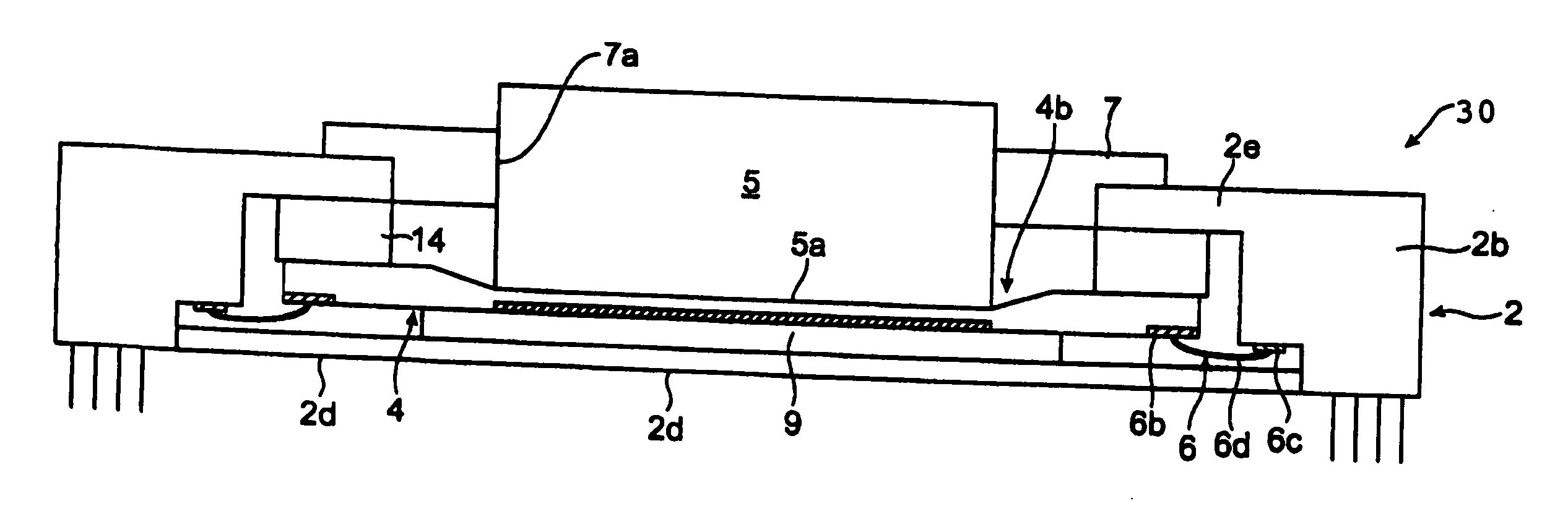
[0084] The arrangement of a third embodiment of an image pickup device according to the present invention shall now be described using FIG. 9.

[0085] The image pickup device 30 according to this third embodiment differs from the first embodiment in the shape of the package 2. The package 2 of this third embodiment has openings at two opposing surfaces. In the following, the opening portion formed on a bottom surface of the package 2 shall be referred to as “bottom surface opening 2g,” and the opening portion formed on an upper end surface of the package 2 shall be referred to as “top plate opening 2f.” With this third embodiment, the bottom surface opening 2g is covered by a bottom cover 2d, and a semiconductor substrate 4 is connected to this bottom cover 2d. That a protective plate 9 is put in contact with a front surface of the semiconductor substrate 4, at which a CCD reading part 4a is formed, is also a point of difference with respect to the first embodiment.

[0086] The princi...


PUM


Abstract

The present invention relates to an image pickup device, etc., having a structure such that electrostatic discharge is unlikely to occur when an FOP and a CCD reading part are joined. This image pickup device comprises a semiconductor substrate, provided with the CCD reading part on a front surface that opposes a back surface, which serves as a light-incident surface, a package having a cavity in which the semiconductor substrate is fixed, a cover covering an upper opening of the cavity, an FOP joined to the semiconductor substrate, and electrical wirings. The cover has a guiding opening for inserting the FOP into the cavity, and the semiconductor substrate is thinned at a portion corresponding to a region at which the CCD reading part is disposed. Also, the semiconductor substrate is fixed to a bottom surface of the cavity such that the CCD reading part and the bottom surface face each other, and a light outgoing end surface of the FOP is optically coupled to the thin part of the semiconductor substrate in the state of being inserted into the cavity from the guiding opening.

Description

TECHNICAL FIELD [0001] The present invention relates to an image pickup device, incorporating a CCD reading part, and a method of manufacturing such an image pickup device. BACKGROUND ART [0002] With a transmission electron microscope, etc., an image pickup device, incorporating a charge reading part (referred to hereinafter as “CCD reading part”) that comprises a charge coupled device, is applied as a means of observing and recording electron beam images. Since a CCD reading part can record images as electronic information, image pickup devices, incorporating such CCD reading parts, have become widely popular in recent years. [0003] As an example of such a conventional image pickup device, the image pickup device described in Japanese Patent Application Laid-Open No. 2000-324400 is known. As shown in FIG. 1, this image pickup device is equipped with a scintillator 107, a semiconductor substrate 109, a fiber optic plate 108 (referred to hereinafter as “FOP”), a CCD reading part cont...

Claims


Application Information

Patent Timeline
Patent Type & Authority Applications(United States)
IPC IPC(8): H01L21/00G01T1/20H01J37/22H01J37/244H01J37/26H01L27/14H01L27/148H04N5/225H04N5/335H04N5/372
CPCH01J37/224H01J37/244H01J2237/2443H01J2237/2445H01L27/14618H01L27/14806H04N5/2254H01L2924/15153H01L2924/15165H01L2924/15312H01L2924/15787H01L2924/19107H04N5/2253H01L31/0203H04N23/54H04N23/55
Inventor KOBAYASHI, HIROYAMURAMATSU, MASAHARU
Owner HAMAMATSU PHOTONICS KK
Why Eureka
Try Eureka