Electro-optical device, method of manufacturing electro-optical device, and electronic apparatus

a manufacturing method and electrooptical technology, applied in the direction of electrical equipment, semiconductor devices, instruments, etc., can solve the problems of lowering manufacturing yields and complicated manufacturing methods, and achieve the effects of improving contrast ratio, high quality image display, and simplifying manufacturing processes

Inactive Publication Date: 2006-11-02
SEIKO EPSON CORP
View PDF13 Cites 15 Cited by
  • Summary
  • Abstract
  • Description
  • Claims
  • Application Information

AI Technical Summary

Benefits of technology

[0033] According to this exemplary embodiment, the above-mentioned electro-optical device can be manufactured. In particular, since the data line composed of the conductive light shielding film is formed on the first interlayer insulating film which has been subjected to the planarizing process, the light leak current in the thin film transistor can be reduced, so that the contrast ratio can be improved, which results in a high quality image display. Further, since the laminated structure on the substrate is relatively simple, the manufacturing process can be simplified, so that the manufacturing yield can be improved. Furthermore, in the process of manufacturing the storage capacitor, the fixed potential side electrode, the dielectric film, and the pixel potential side electrode may be sequentially laminated in this order or may be laminated in reverse order.

Problems solved by technology

However, according to the various technologies in this field, a laminated structure on the substrate becomes complicated in achieving a high function or a high performance, which results in complicated manufacturing methods and lowering manufacturing yields.

Method used


Image

  • Electro-optical device, method of manufacturing electro-optical device, and electronic apparatus
  • Electro-optical device, method of manufacturing electro-optical device, and electronic apparatus
  • Electro-optical device, method of manufacturing electro-optical device, and electronic apparatus

Examples


Embodiment Construction

[0051] Hereinafter, preferred embodiments of the invention will be described in detail with reference to accompanying drawings. In the exemplary embodiments which will be described in detail below, a driving circuit-built TFT active-matrix-driving-type liquid crystal device, which is an example of an electro-optical device according to one embodiment of the invention, will be exemplified.

[0052] A liquid crystal device according to a first exemplary embodiment of the invention will be described in detail with reference to FIGS. 1 to 9.

Structure of Electro-Optical Device

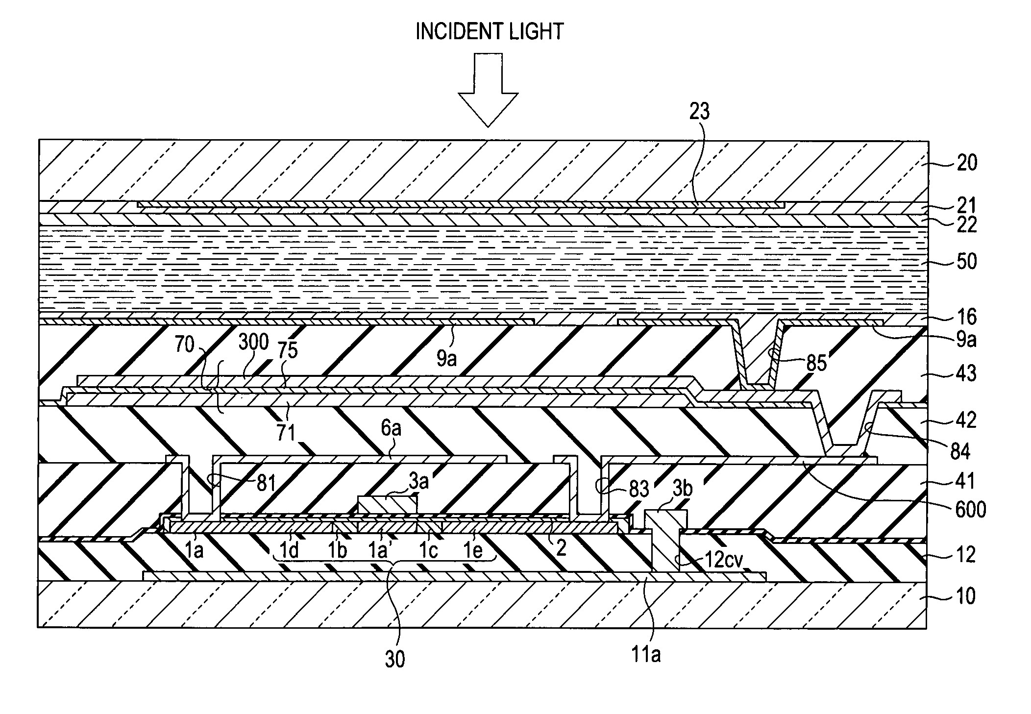
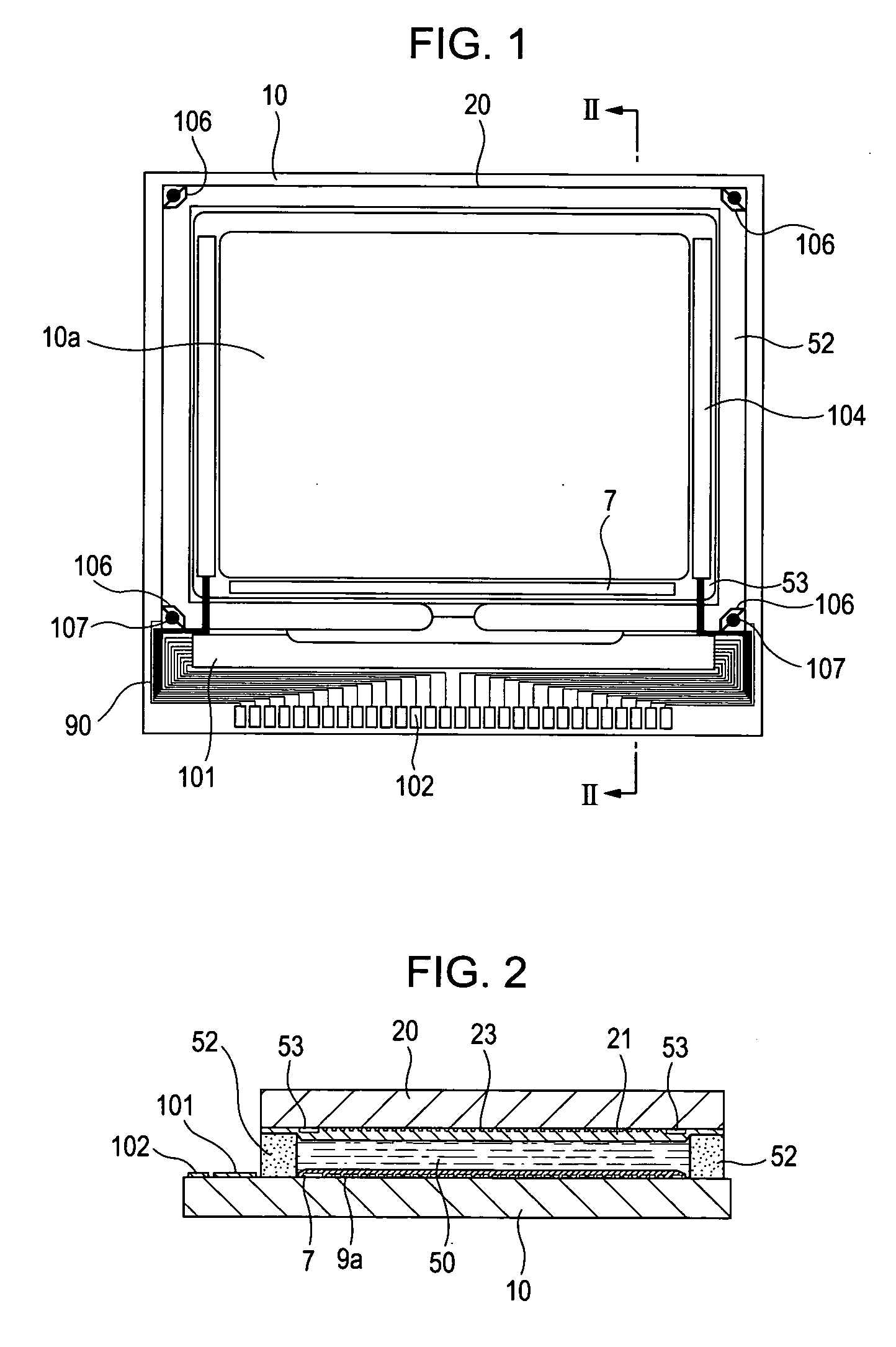
[0053] First, the structure of a liquid crystal device according to the an exemplary embodiment will be described with reference to FIGS. 1 and 2. FIG. 1 is a plan view illustrating a structure of the liquid crystal device according to the an embodiment of the invention, and FIG. 2 is a cross-sectional view taken along the line II-II of FIG. 1.

[0054] In FIGS. 1 and 2, in the liquid crystal device according to one ...


PUM


Abstract

An electro-optical device comprising thin film transistors disposed closer to a substrate than data lines and a first interlayer insulating film that is laminated on the thin film transistors and is subjected to a planarizing process. Storage capacitors are disposed further from the substrate than the data lines, and each storage capacitor includes a fixed potential side electrode, a dielectric film, and a pixel potential side electrode. Pixel electrodes are disposed further from the substrate than the storage capacitors and are electrically connected to the pixel potential side electrode and the thin film transistor. Each of the data lines comprises a conductive light shielding film which is formed so as to at least partially cover the channel region of each of the thin film transistors in plan view.

Description

RELATED APPLICATION INFORMATION [0001] The present application claims priority from Japanese Patent Application No. 2005-113146, filed on Apr. 11, 2005, and Japanese Patent Application No. 2006-020094, filed on Jan. 30, 2006, the entire contents of which are hereby incorporated by reference. BACKGROUND [0002] 1. Technical Field [0003] The present invention relates to an electro-optical device, such as a liquid crystal device, to a method of manufacturing an electro-optical device, and to an electronic apparatus, such as a liquid crystal projector. [0004] 2. Related Art [0005] In general, an electro-optical device includes pixel electrodes, scanning lines that selectively drive the corresponding pixel electrodes, data lines, and thin-film transistors (TFTs) serving as pixel switching elements, all of which are formed on a substrate. The electro-optical device is constructed such that active matrix driving can be performed. Further, in order to achieve a high contrast ratio, a storage...

Claims


Application Information

Patent Timeline
Patent Type & Authority Applications(United States)
IPC IPC(8): H01L29/04
CPCH01L29/78633H01L27/124H01L27/1255H10K59/126H10K59/131G02F1/136
Inventor YAMASAKI, YASUJI
Owner SEIKO EPSON CORP
Why Eureka
Try Eureka