Gallium-nitride based light emitting diode structure and fabrication thereof

a light-emitting diode and gallium-nitride technology, applied in the direction of semiconductor devices, electrical apparatus, transistors, etc., can solve the problems of ineffective utilization, inability to effectively utilize, and inherently limited light-emitting efficiency of conventional gan-based leds, and achieve superior conductivity

Inactive Publication Date: 2006-11-02
SEMILEDS OPTOELECTRONICS CO LTD
View PDF7 Cites 1 Cited by
  • Summary
  • Abstract
  • Description
  • Claims
  • Application Information

AI Technical Summary

Benefits of technology

[0012] The present invention provides a new structure for the p-type transparent metallic conductive layer. The present invention first forms a first contact spreading metallic layer on top of the texturing surface of the p-type ohmic contact layer. The present invention then forms a second and third contact spreading metallic layers on top of the first contact spreading metallic layer. The three-layered p-type transparent metallic conductive layer is alloyed under a high temperature within an oxygenic or nitrogenous environment and has a superior conductivity.
[0013] For GaN-based LEDs fabricated according to the present invention, the first contact spreading metallic layer is extremely thin so that lights emitted out of the active layer are neither absorbed nor reflected. The first contact spreading metallic layer could also enhance the lateral contact uniformity between the p-type metallic electrode and the p-type GaN ohmic contact layer, so as to avoid the localized light emission resulted from the uneven distribution of the second contact spreading metallic layer within the third contact spreading metallic layer. The GaN-based LED's working voltage and external quantum efficiency are also significantly improved.
[0014] The fabrication method according to the present invention does not have a mechanism to cause the first contact spreading layer to have an uneven lateral distribution under a high temperature. The GaN-based LED's characteristics and stability are thereby preserved.

Problems solved by technology

The 75% of the lights also have a high probability to be absorbed again after undergoing multiple reflections within the LED and, therefore, cannot be effectively utilized.
In other words, the light emitting efficiency of the conventional GaN-based LED is inherently limited by the re-absorption of the transparent metallic conductive layer and the LED's internal epitaxial structure.
This would cause uneven lateral distribution of electrical current, localized light emission, and increase of working voltage.

Method used


Image

  • Gallium-nitride based light emitting diode structure and fabrication thereof
  • Gallium-nitride based light emitting diode structure and fabrication thereof
  • Gallium-nitride based light emitting diode structure and fabrication thereof

Examples


Embodiment Construction

[0021] In the following, detailed description along with the accompanied drawings is given to better explain preferred embodiments of the present invention. Please be noted that, in the accompanied drawings, some parts are not drawn to scale or are somewhat exaggerated, so that people skilled in the art can better understand the principles of the present invention.

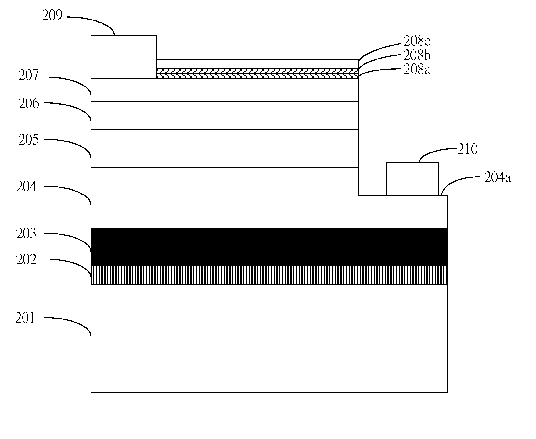
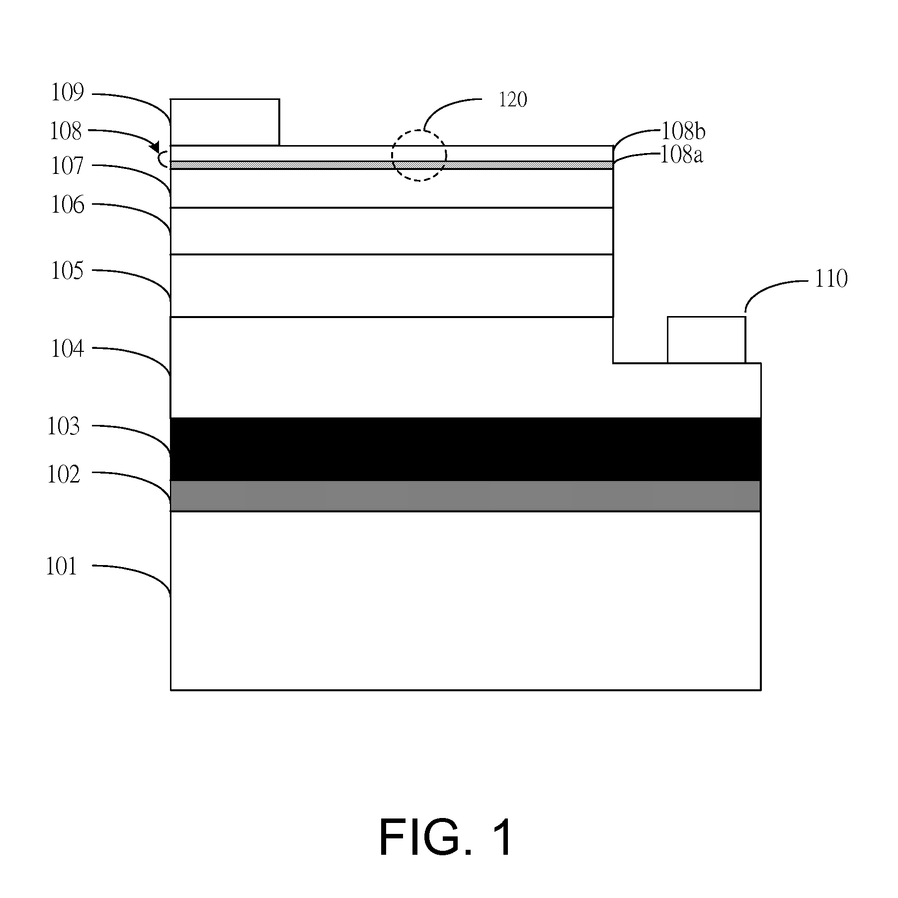
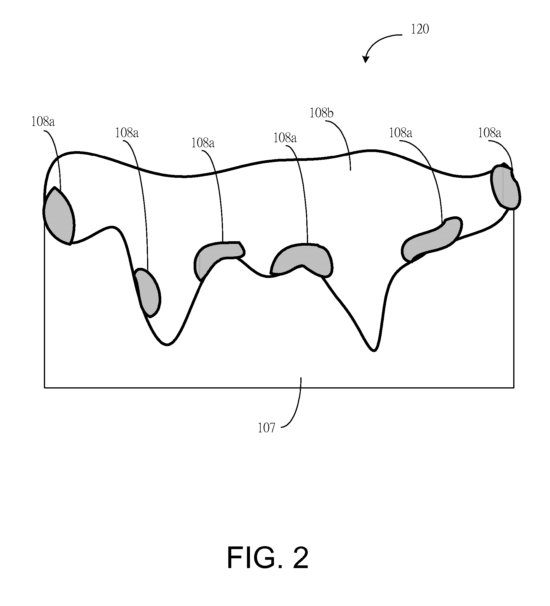
[0022] FIGS. 3(a)-3(d) are schematic diagrams showing the epitaxial structure of a GaN-based LED after the processing steps of the present invention respectively.

[0023] As shown in FIG. 3(a), a sapphire substrate 201 is provided. Then, on top of the substrate 201, a number of GaN-based epitaxial layers are developed. The material used for forming these epitaxial layers could be described by the following molecular formulas:

BxAlyInzGa1-x-y-zNpASq; and

BxAlyInzGa1-x-y-zNpPq,

where 0≦x≦1, 0≦y≦1, 0≦z≦1, 0≦p≦1, 0≦q≦1, and x+y+z=1, p+q=1.

[0024] The epitaxial layers are developed as follows. A low-temperature buffer layer 202...


PUM

PropertyMeasurementUnit
temperatureaaaaaaaaaa
resistivity coefficientaaaaaaaaaa

Abstract

A method for fabricating GaN-based LED is provided. The method first forms a first contact spreading metallic layer on top of the texturing surface of the p-type ohmic contact layer. The method then forms a second and a third contact spreading metallic layers on top of the first contact spreading layer. The p-type transparent metallic conductive layer composed of the three contact spreading metallic layers, after undergoing an alloying process within an oxygenic or nitrogenous environment under a high temperature, would have a superior conductivity. The p-type transparent metallic conductive layer could enhance the lateral contact uniformity between the p-type metallic electrode and the p-type ohmic contact layer, so as to avoid the localized light emission resulted from the uneven distribution of the second contact spreading metallic layer within the third contact spreading metallic layer. The GaN-based LED's working voltage and external quantum efficiency are also significantly improved.

Description

CROSS-REFERENCES TO RELATED APPLICATIONS [0001] This is a division of U.S. application Ser. No. 11 / 020,737, filed Dec. 22, 2004.BACKGROUND OF THE INVENTION [0002] 1. Field of the Invention [0003] The present invention generally relates to gallium-nitride based light emitting diodes and, more particularly, to the structure and fabrication method of a transparent metallic conductive layer for enhancing the gallium-nitride based light emitting diodes' luminous uniformity. [0004]2. The Prior Arts [0005] A gallium-nitride (GaN) based light-emitting diode (LED) having a conventional structure as shown in FIG. 1 is usually grown on a sapphire substrate. The conventional GaN-based LED contains a number of GaN-based epitaxial layers on top of a side of the sapphire substrate 101. These epitaxial layers are sequentially stacked from bottom to top in the following order on the sapphire substrate 101: a low-temperature GaN buffer layer 102, a high-temperature GaN buffer layer 103, an n-type GaN...

Claims


Application Information

Patent Timeline
Patent Type & Authority Applications(United States)
IPC IPC(8): H01L29/80H01L31/112H01L27/15H01L33/12H01L33/32H01L33/42
CPCH01L33/42H01L33/32
Inventor LAI, MU-JENHON, SCHANG-JING
Owner SEMILEDS OPTOELECTRONICS CO LTD
Why Eureka
Try Eureka