Optical element device and two-dimensional optical waveguide device and optoelectronic circuit board using the same

a technology of optical waveguide and optical element, which is applied in the direction of optical elements, optical waveguide light guides, instruments, etc., can solve the problems of difficult mounting of light emitting elements, limited light emitting elements and light receiving elements, and signal delays and emis, so as to achieve efficient optical couplement, facilitate mounting, and facilitate the effect of rearranging the optical signal transmitting region

Inactive Publication Date: 2006-11-02
CANON KK
View PDF20 Cites 15 Cited by
  • Summary
  • Abstract
  • Description
  • Claims
  • Application Information

AI Technical Summary

Benefits of technology

[0024] An optical element device comprising an optical path transforming structure as well as a light emitting device and / or light receiving device can efficiently optically couple the optical element(s) with the optical waveguide and the optical element(s) can be easily mounted in a two-dimensional optical waveguide layer. Additionally, when transmitting an optical signal through a two-dimensional optical waveguide device comprising an optical element device according to the invention, the optical signal transmitting region can be restructured with ease.

Problems solved by technology

Compact, lightweight and functionally sophisticated devices of the type under consideration entail development of high speed operating circuit boards and an enhanced level of integration, which by turn give rise to various problems including signal delays and EMIs (electromagnetic interferences).
However, because optical wiring provides a transmission line (linear polymer waveguide), the site for electric / optical signal conversion or optical / electric signal conversion can automatically be defined and hence is limited.
On the other hand, with the technique as disclosed in Japanese Patent Application Laid-Open No. 2000-199827, it can be difficult to mount a light emitting element on a linear optical waveguide having at an end thereof a mirror that is inclined by 45° so as to efficiently couple optical signals and to mount a light receiving element on the linear optical waveguide so as to efficiently receive an optical signal propagated through the latter because such a technique requires a high alignment accuracy.
Additionally, because the technique involves the use of a linear optical waveguide, the position of the light emitting element and that of the light receiving element can be restricted to reduce the design freedom particularly when a plurality of optical waveguides need to be formed.

Method used


Image

  • Optical element device and two-dimensional optical waveguide device and optoelectronic circuit board using the same
  • Optical element device and two-dimensional optical waveguide device and optoelectronic circuit board using the same
  • Optical element device and two-dimensional optical waveguide device and optoelectronic circuit board using the same

Examples


embodiment 1

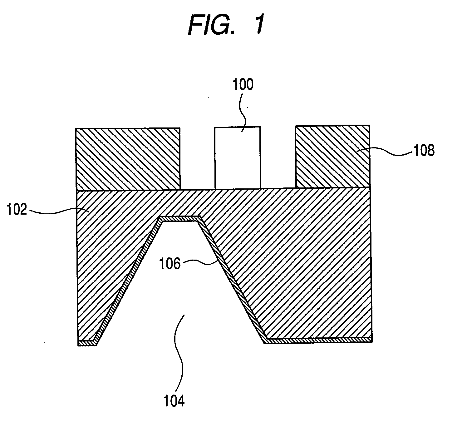
[0038]FIG. 1 is a schematic cross sectional view of the first embodiment of the present invention, which is a light emitting element device comprising a surface emission type light emitting element. In FIG. 1, there are shown a surface emission type light emitting element 100 (VCSEL: vertical cavity surface emitting laser), which is a functional section of the light emitting element device, a growth substrate 102, an optical path transforming structure 104, a metal film (mirror) 106 of the optical path transforming structure 104 and a semiconductor layer 108. The surface emission type light emitting element 100, which is a functional section of the light emitting element device, and the metal film 106 of the optical path transforming structure 104 are arranged to show such a positional relationship that light emitted from the surface emission type light emitting element 100 is coupled to the optical path transforming structure 104 so as to turn the optical path by 90D.

[0039] Now, a...

embodiment 2

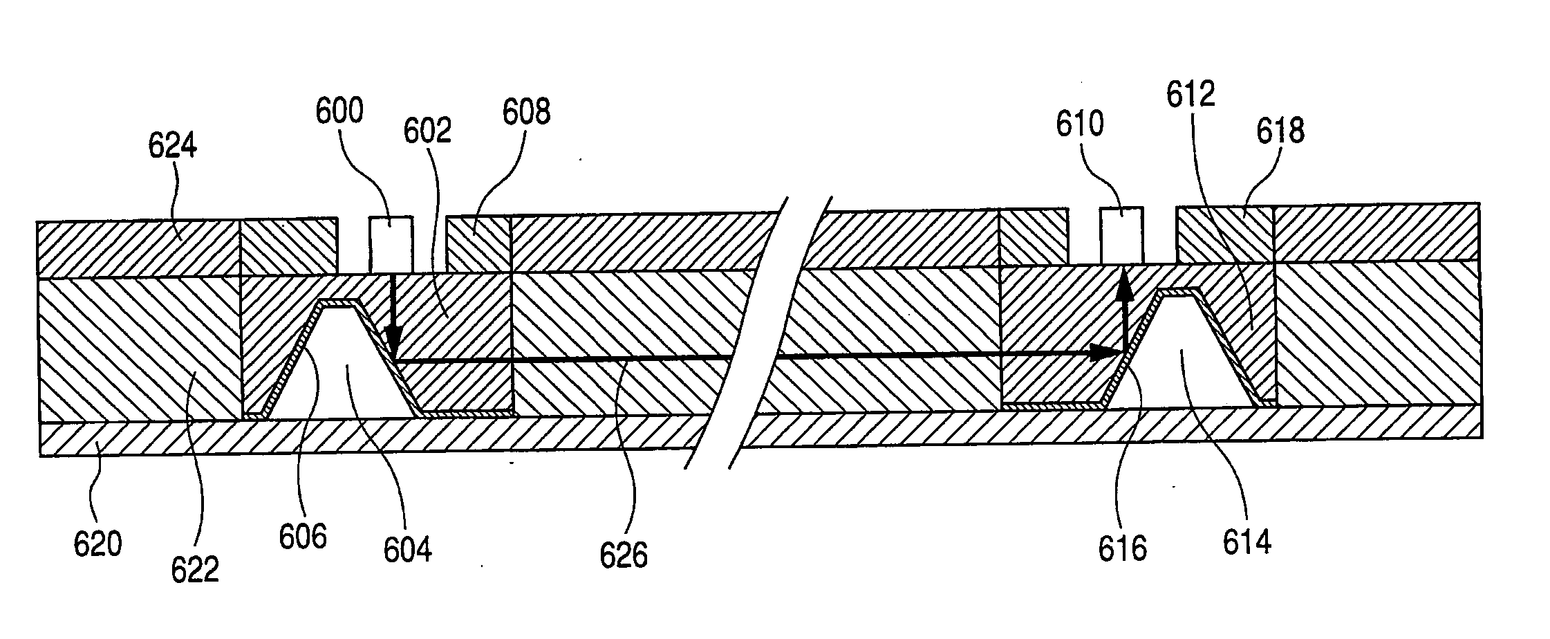
[0050]FIG. 6 is a schematic cross sectional view of the second embodiment of the present invention, which is a two-dimensional optical waveguide device comprising an optical element device including a pair of optical path transforming structures as well a surface emission type light emitting element and a light receiving element integrally formed with it. In FIG. 6, there are shown a surface emission type light emitting element (VCSEL) 600, a pair of growth substrates 602 and 612, a pair of optical path transforming structures 604 and 614, metal films (mirrors) 606 and 616, a pair of semiconductor layers 608 and 618, a light receiving element 610, a first clad layer 620, a core layer 622, a second clad layer 624 and a laser beam 626. The two-dimensional optical waveguide is formed by using a combination of different materials showing respective refractive indexes that are different from each other, that is, by the core layer 622 and the first and second clad layers 620 and 624 that ...

embodiment 3

[0057] The third embodiment is a two-dimensional optical waveguide device in which a surface emission type light emitting element that is integral with an optical path transforming structure and a light receiving element that is also integral with an optical path transforming structure are formed on a same growth substrate while light emitted from the surface emission type light emitting element is propagated through the growth substrate that operates as optical waveguide layer and propagated light is coupled to the light receiving element to transmit an optical signal. FIG. 8 is a schematic cross sectional view of this embodiment of two-dimensional optical waveguide device. In FIG. 8, there are shown a surface emission type light emitting element 800, a growth substrate 802, a pair of optical path transforming structures 804 and 812, a pair of metal films (mirrors) 806 and 814, a semiconductor layer 808 and a light receiving element 810.

[0058] The surface emission type light emitt...


PUM


Abstract

An optical element device comprises an optical element and an optical path transforming structure for changing a light proceeding direction in order to couple light with the optical element or light from said optical element with some other element, in which said optical path transforming structure is formed by processing a substrate where said optical element is formed.

Description

TECHNICAL FIELD [0001] This invention relates to an optical element device (that comprises a light emitting element and / or a light receiving element and an optical path transforming structure integrally formed with such an element). It also relates to a two-dimensional optical waveguide device comprising such an optical element device and an optoelectronic circuit board carrying such a two-dimensional optical waveguide device along with an electric wiring layer and an optical wiring layer. BACKGROUND ART [0002] As mobile phones and personal information terminals are rapidly becoming popular, there is an increasing demand for such devices that are more compact, lightweight and, at the same time, functionally sophisticated. Compact, lightweight and functionally sophisticated devices of the type under consideration entail development of high speed operating circuit boards and an enhanced level of integration, which by turn give rise to various problems including signal delays and EMIs ...

Claims


Application Information

Patent Timeline
Patent Type & Authority Applications(United States)
IPC IPC(8): G02B6/12G02B6/42G02B6/43G02B6/122H01L27/14H01L27/15H05K1/02
CPCG02B6/43G02B6/4214
Inventor UCHIDA, TATSURO
Owner CANON KK
Why Eureka
Try Eureka