Dual pulsed beam laser micromachining method

a laser micromachining and laser scribing technology, applied in the field of micromachining, can solve the problems of affecting the yield and reliability of semiconductor devices, affecting the integration of these ild materials, and being more prone to saw-related scribe line damag

Inactive Publication Date: 2006-11-09
INTEL CORP
View PDF9 Cites 52 Cited by
  • Summary
  • Abstract
  • Description
  • Claims
  • Application Information

AI Technical Summary

Problems solved by technology

However, the integration of these ILD materials is not necessarily a simple matter.
More specifically, because low-k dielectric materials are mechanically weaker than conventional silicon dioxide, they are more prone to saw-related scribe line damage, such as cracks.
To the extent that this damage propagates to other areas of the wafer, semiconductor device yields and reliability can be compromised.
Lasers, however, are not without process integration issues.
H...

Method used


Image

  • Dual pulsed beam laser micromachining method
  • Dual pulsed beam laser micromachining method
  • Dual pulsed beam laser micromachining method

Examples


Embodiment Construction

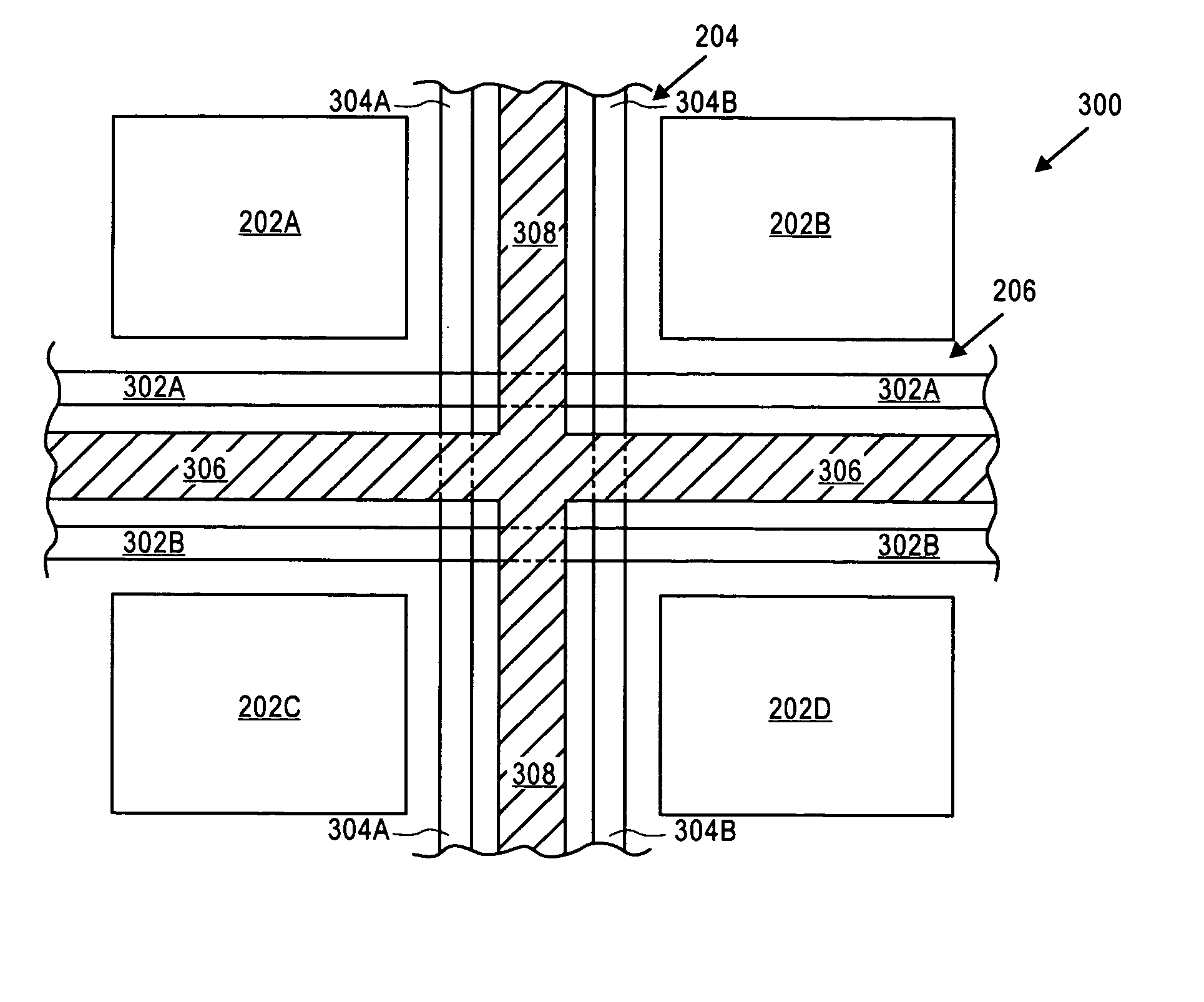
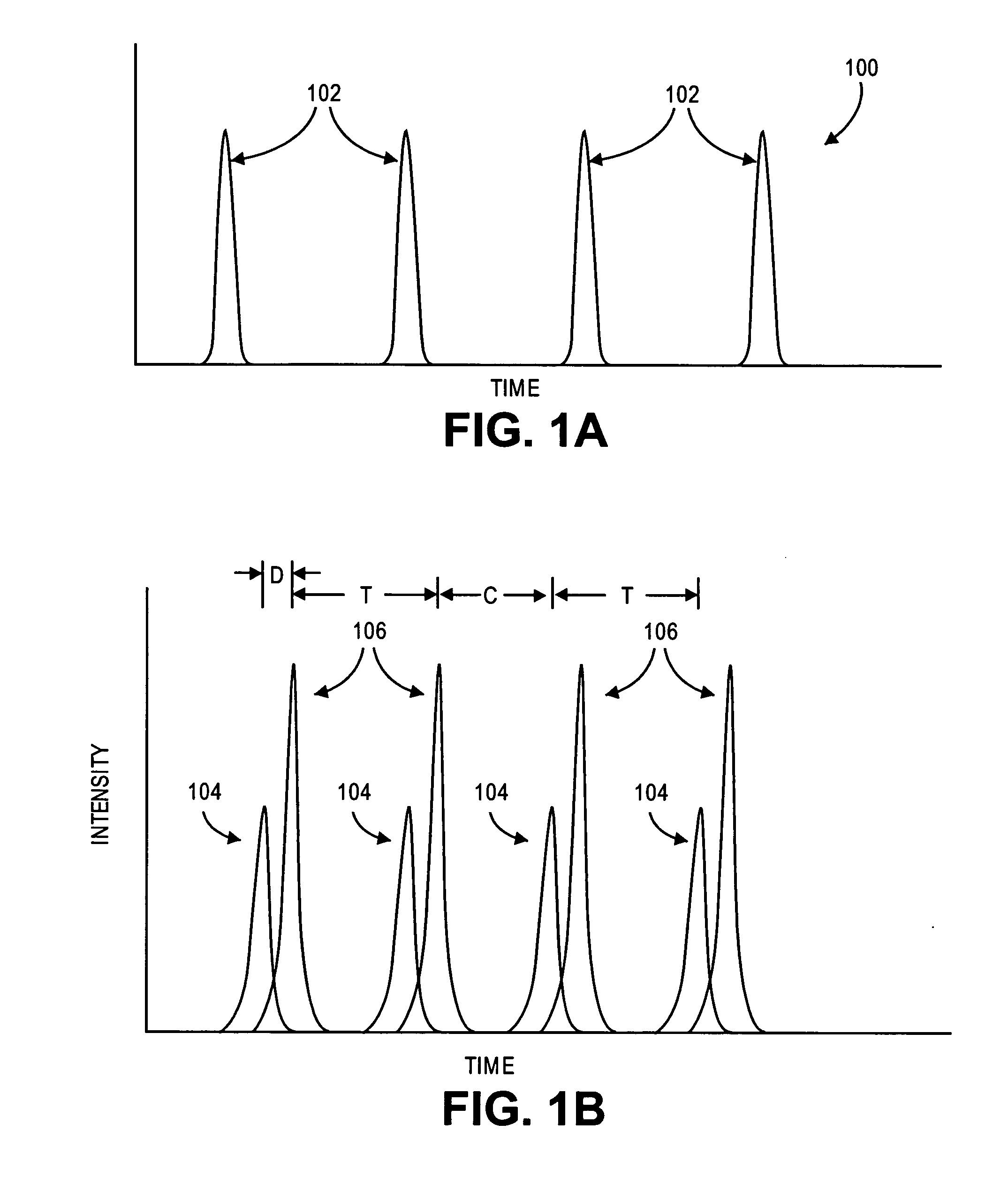
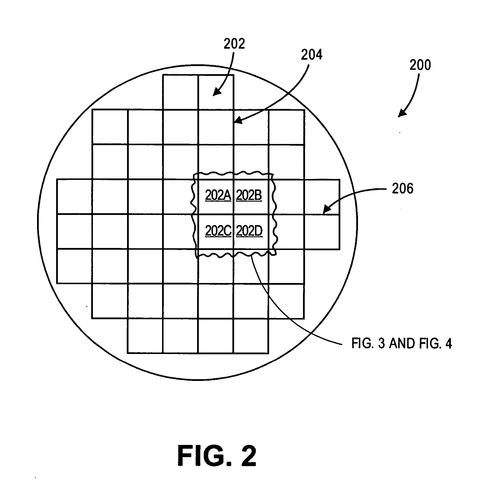
[0013] In the following detailed description, a method for laser micromachining a workpiece is disclosed. Reference is made to the accompanying drawings within which are shown, by way of illustration, specific embodiments by which the present invention may be practiced. It is to be understood that other embodiments may exist and that other structural changes may be made without departing from the scope and spirit of the present invention.

[0014] The terms on, above, below, and adjacent as used herein refer to the position of one layer or element relative to other layers or elements. As such, a first element disposed on, above, or below a second element may be directly in contact with the second element or it may include one or more intervening elements. In addition, a first element disposed next to or adjacent a second element may be directly in contact with the second element or it may include one or more intervening elements.

[0015] Embodiments of the present invention relate gene...


PUM

PropertyMeasurementUnit
Nanoscale particle sizeaaaaaaaaaa
Lengthaaaaaaaaaa
Timeaaaaaaaaaa

Abstract

A method is described for laser scribing or dicing portions of a workpiece using multi-source laser systems. In one embodiment, a first laser melts portions of the workpiece prior to a second laser ablating the portions of the workpiece.

Description

FIELD OF THE INVENTION [0001] Embodiments of the present invention relate generally to micromachining and more specifically to the laser scribing of semiconductor substrates. BACKGROUND OF THE INVENTION [0002] The need to use low dielectric constant (low-k) interlayer dielectric (ILD) materials in scaled semiconductor devices is becoming necessary to reduce line-to-line capacitive coupling effects. However, the integration of these ILD materials is not necessarily a simple matter. One place this is evident is at the wafer saw / singulation process. [0003] More specifically, because low-k dielectric materials are mechanically weaker than conventional silicon dioxide, they are more prone to saw-related scribe line damage, such as cracks. To the extent that this damage propagates to other areas of the wafer, semiconductor device yields and reliability can be compromised. This problem has been addressed by some manufacturers by first using a laser to scribe through the material formed ove...

Claims


Application Information

Patent Timeline
IPC IPC(8): H01L29/06B23K26/00H01L21/78
CPCB23K26/0604B23K26/0613B23K26/063H01L21/78B23K2201/40H01L21/268B23K26/4075B23K26/40B23K26/0622B23K2101/40B23K2103/50
Inventor LI, ERIC J.VORONOV, SERGEI L.RUMER, CHRISTOPHER L.
Owner INTEL CORP
Why Eureka
Try Eureka