Semiconductor device, circuit board, and electronic instrument

Inactive Publication Date: 2006-11-09
SEIKO EPSON CORP
View PDF34 Cites 2 Cited by
  • Summary
  • Abstract
  • Description
  • Claims
  • Application Information

AI Technical Summary

Benefits of technology

[0014] Besides, since the conducting portions between the electrodes and the external electrodes can be formed freely according to the requirements of the design, the layout of the external electrodes can be determined regardless of the layout of the electrodes. As a result, without changing the circuit design of the elements formed on the wafer, various semiconductor devices with the external electrodes in different positions can easily be fabricated.
[0

Problems solved by technology

However, for bare chips, quality control and handling are difficult.
However, in cases wh

Method used


Image

  • Semiconductor device, circuit board, and electronic instrument
  • Semiconductor device, circuit board, and electronic instrument
  • Semiconductor device, circuit board, and electronic instrument

Examples


first embodiment

[0145] The present invention seeks to further improve on the above described basic art, and the present invention is now described in terms of a number of preferred embodiments, with reference to the drawings.

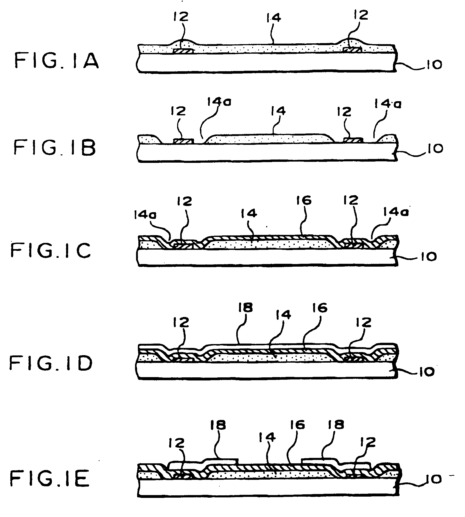
[0146]FIGS. 14A to 14D illustrate a first embodiment of the present invention.

[0147] In the semiconductor device 150 shown in FIG. 14A, a resin layer 152 of polyimide is formed discontinuously. The resin layer 152 forms a stress relieving layer. As a stress relieving layer, photosensitive polyimide resin is preferable, but a nonphotoaensitive resin may also be used. A material such as a silicone denatured polyimide resin, an epoxy resin, or a silicone denatured epoxy resin that has a stress relieving function having a low Young's modulus (not exceeding 1×10¹⁶ Pa) when solidified may be used.

[0148] Besides, in the resin layer 152 is formed a tapered depression 152a. Then wiring 154 is formed along the surface shape of the depression 152a, as a result of which, the wiring 154 ...

second embodiment

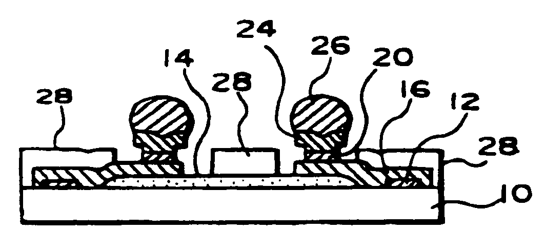
[0156] Next, the semiconductor device 190 shown in FIG. 15 is characterized by wiring 200 connecting an aluminum pad 192 and a solder ball 196 provided on a stress relieving layer 194. For the wiring 200 may be used any of the wiring materials selected for the first basic art and the like. This wiring 200 has a bellows-like portion 200a. The bellows-like portion 200a, as shown in FIG. 14D, is in a state that wire includes a slit and a plurality of the bellows-like portion 200a is continuously formed between normal wiring. The bellows-like portion200a has better stress-absorbing properties than the bent wiring 184. By the provision of the bellows-like portion 200a, the occurrence of cracks in the wiring 200 on the semiconductor chip, and damage to the aluminum pad 192 and other active elements is eliminated, and the reliability of the semiconductor device is increased. Besides, since the bellows-like portion 200a is provided in a single wiring, the space required for the stress absor...

third embodiment

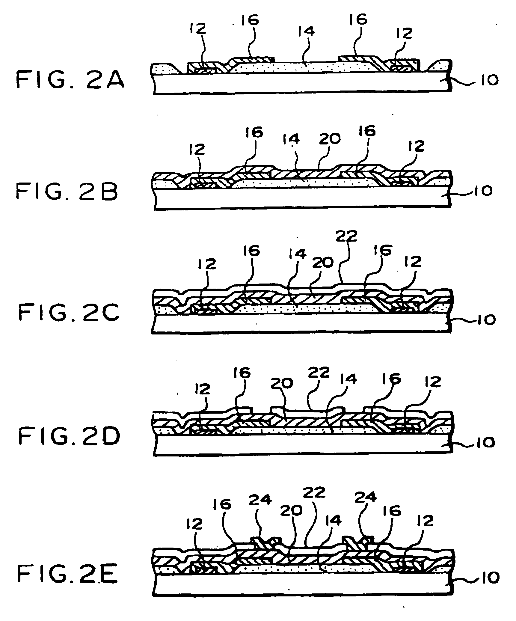
[0158] FIGS. 16 to 20 show a third embodiment of the present invention. FIG. 16 shows a cross-section of the semiconductor device of this embodiment. A semiconductor device 300 has a semiconductor chip 302 on which is a multi-layer structure (four layers), and the surface being protected by a solder resist 350. It should be noted that in this embodiment also, materials and manufacturing method, and so on described in other embodiments and in the basic art, may also be applied.

[0159]FIGS. 17A and 17B show the first layer. In more detail, FIG. 17B is a plan view and FIG. 17A is a cross-sectional view along the line VII-VII in FIG. 178. The semiconductor chip 302 has an electrode 304 which inputs or outputs a signal. A stress relieving layer 310 is formed to be inclined at the end thereof, in the vicinity of the electrode. The stress relieving layer 310 is an insulator, and in particular a polyimide resin is preferable. Next, signal wiring 312 is formed from the electrode 304 to over ...


PUM


Abstract

A semiconductor device with a package size close to its chip size is, apart from a stress absorbing layer, such as to effectively absorb thermal stresses. A semiconductor device (150) has a semiconductor chip provided with electrodes (158), a resin layer (152) forming a stress relieving layer provided on the semiconductor chip, wiring (154) formed from the electrodes (158) to over the resin layer (152), and solder balls (157) formed on the wiring (154) over the resin layer (152); the resin layer (152) is formed so as to have a depression (152a) in the surface, and the wiring (154) is formed so as to pass over the depression (152a).

Description

[0001] This is a Division of application Ser. No. 10 / 463,470 filed Jun. 18, 2003, which in turn is a Continuation of application Ser. No. 09 / 666,406 (now U.S. Pat. No. 6,608,389), which in turn is a Continuation of application Ser. No. 09 / 117,526 (now U.S. Pat. No. 6,255,737), which is the National Stage of International Application No. PCT / JP97 / 04438 filed Dec. 4, 1997. The entire disclosure of the prior applications is hereby incorporated by reference herein in its entirety.TECHNICAL FIELD [0002] The present invention relates to a semiconductor device and method of making the same, a circuit board, and an electronic instrument, and in particular relates to a semiconductor device having a package size close to the chip size and a method of making the same, a circuit board, and an electronic instrument. BACKGROUND ART [0003] To pursue high-density mounting in semiconductor devices, bare chip mounting is the ideal. However, for bare chips, quality control and handling are difficult. ...

Claims


Application Information

Patent Timeline
IPC IPC(8): H01L23/48H01L21/60H01L21/768H01L23/31H01L23/36H01L23/485H01L23/532
CPCH01L21/768H01L2224/0401H01L23/3171H01L23/36H01L23/525H01L23/5329H01L24/11H01L2224/0231H01L2224/13099H01L2224/16H01L2924/01002H01L2924/01004H01L2924/01013H01L2924/01022H01L2924/01029H01L2924/01033H01L2924/01056H01L2924/01074H01L2924/01078H01L2924/01079H01L2924/01082H01L2924/014H01L2924/09701H01L2924/19041H01L2924/19043H01L2924/3011H01L24/13H01L2924/01005H01L2924/01006H01L2924/01024H01L23/3114H01L2924/0001H01L2224/13144H01L2224/131H01L2924/00014H01L2924/351H01L2924/12042H01L2224/13022H01L2224/05647H01L2224/02351H01L2224/0236H01L2224/05548H01L2224/02377H01L24/05H01L2924/00H01L21/3205
Inventor HASHIMOTO, NOBUAKI
Owner SEIKO EPSON CORP
Why Eureka
Try Eureka