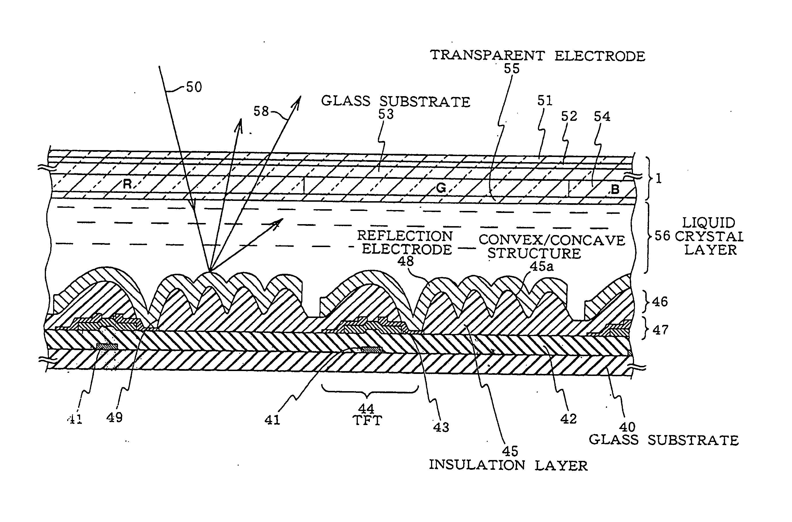
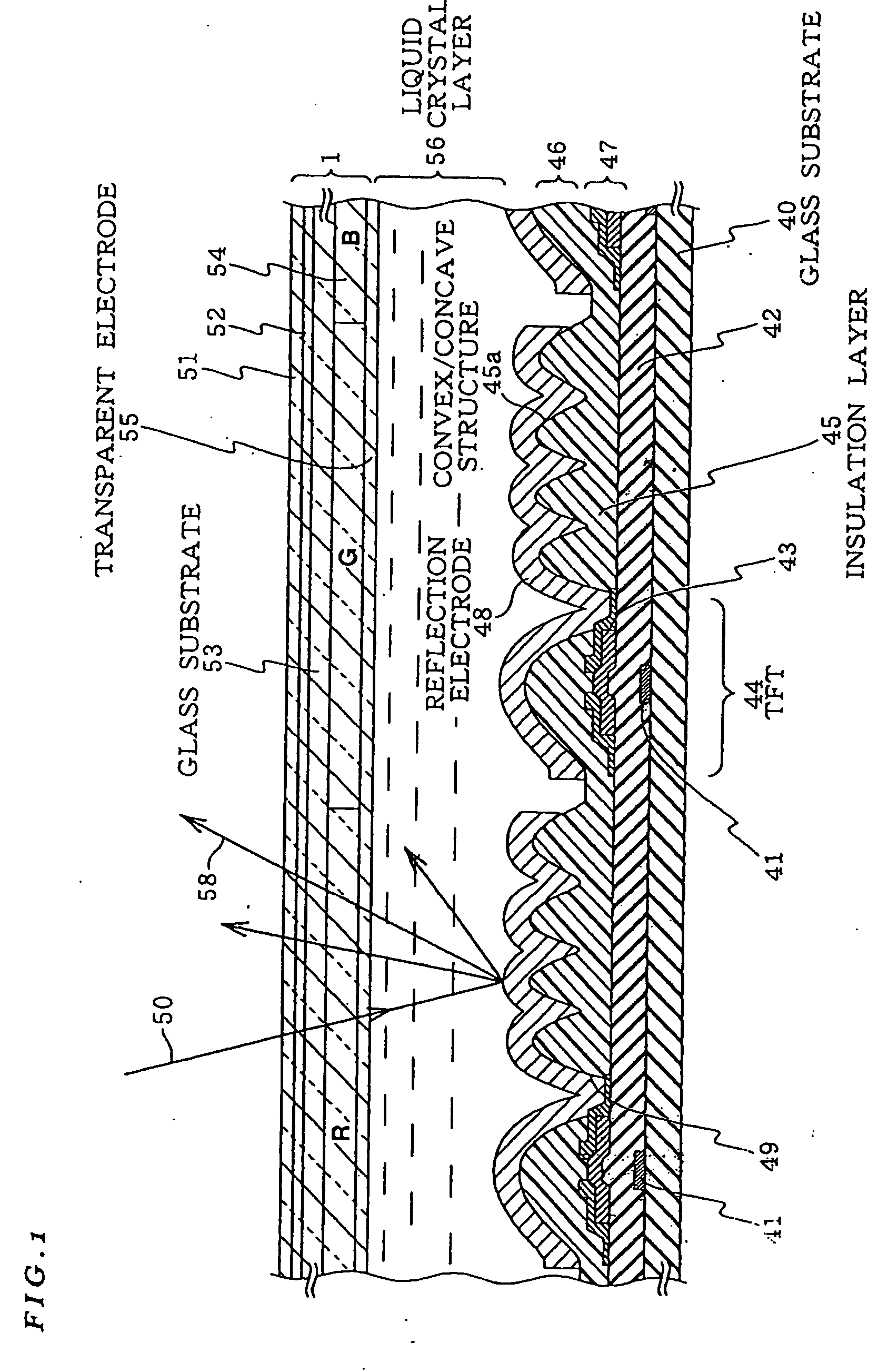
Reflective liquid crystal display apparatus and production method thereof
a liquid crystal display and reflector technology, applied in the direction of identification means, instruments, non-linear optics, etc., can solve problems such as deterioration of switching elements, and achieve the effect of simplifying production procedures
- Summary
- Abstract
- Description
- Claims
- Application Information
AI Technical Summary
Benefits of technology
Problems solved by technology
Method used
Image

Examples
example 1
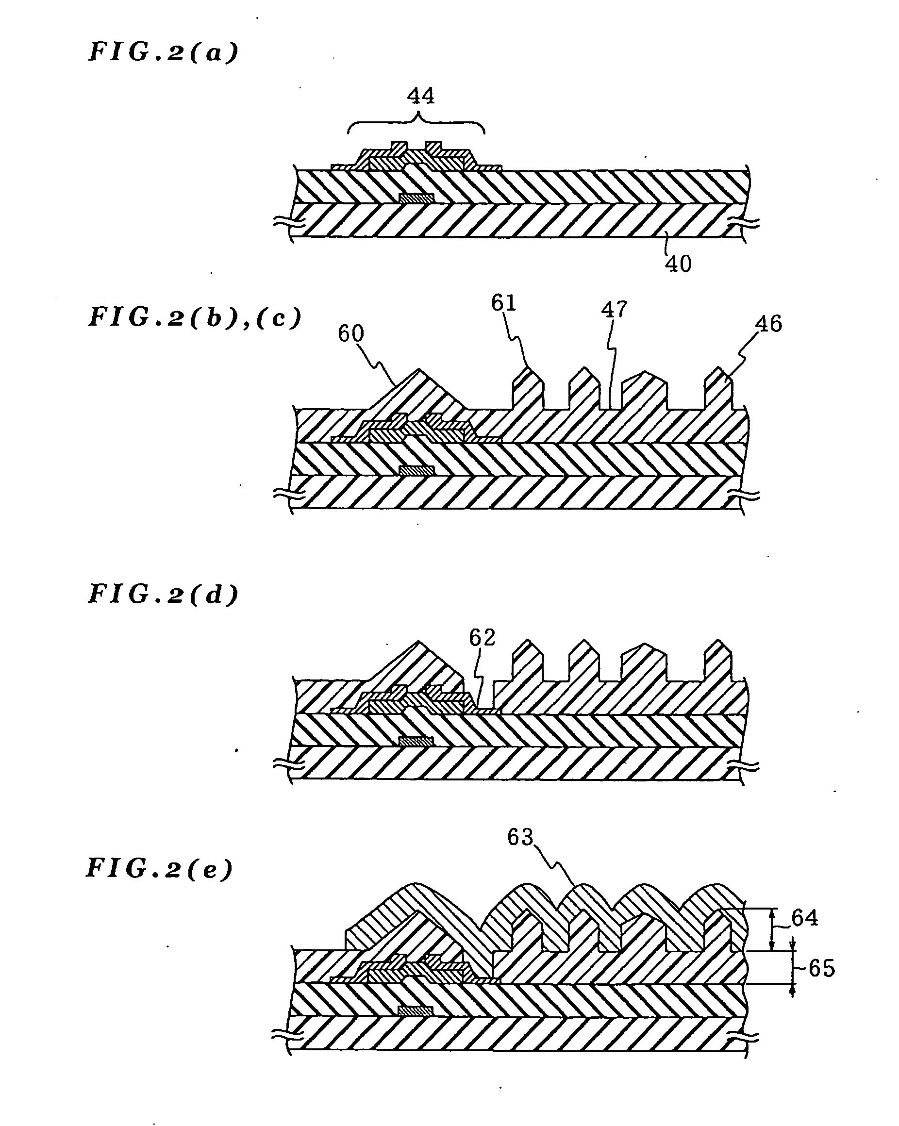
[0135]FIG. 22 and FIG. 23 show production steps for producing a reflective LCD apparatus in this example. As a switching element, a thin film transistor of forward stagger structure was used.
[0136] The production was performed by following production steps on a glass substrate.
[0137] [a] formation of an ITO film with 50 nm thickness by sputtering
[0138] [b] formation of a source 200 and a drain electrode 201 (using 1st photoresist)
[0139] [c] use of plasma CVD to form a doping layer 202 with 100 nm thickness, a semiconductor layer 203 with 100 nm thickness, and a gate insulation film 204 with 400 nm thickness
[0140] [d] formation of a Cr layer 205 with 50 nm thickness by sputtering
[0141] [e] formation of a gate electrode and an island 206 of the TFT element portion (using 2nd photoresisit)
[0142] [f] formation of an organic insulation film 207 (3 micrometers)
[0143] [g] formation of a convex / concave pattern 208 on the upper layer of the organic insulation film (using 3rd photores...
example 2
[0160]FIG. 25 and FIG. 26 show production steps for producing a reflective LCD apparatus used in Example 2. For the switching element in this reflective LCD apparatus, a thin film transistor of inverse stagger configuration was used.
[0161] The production was performed on the glass substrate 230 through following steps.
[0162] [a] formation of Cr film of 50 nm thickness by sputtering
[0163] [b] formation of a gate electrode 231 (1st photoresist)
[0164] [c] formation of a gate insulation film 232 of 400 nm thickness, a semiconductor layer 233 of 100 nm thickness, and a doping layer 234 of 100 nm thickness by using the CVD method
[0165] [d] formation of an island 235 (2nd photoresist)
[0166] [e] formation of a Cr layer and an ITO layer by sputtering
[0167] [f] formation of a source electrode 236 and a drain electrode 237 (3rd photoresist)
[0168] [g] formation of an organic insulation film 238 (3 micrometers)
[0169] [h] formation of a convex / concave pattern 239 in the upper layer porti...
example 3
[0178] In this example, the convex / concave surface under the reflective electrode has a smooth convex / concave configuration. FIG. 28 and FIG. 29 are cross sectional views of the reflective LCD apparatus produced in this example.
[0179] This example is identical to Example 1 and Example 2 except for that an additional step is performed for converting the protrusions / indentations under the reflection electrode into a smooth shape. More specifically, a step for applying a thermal treatment is added after the step [i] in Example 1 and after the step [h] in Example 2. Accordingly, FIG. 28 is identical to FIG. 25.
[0180] In this example, the thermal treatment after the formation of the protrusions / indentations was performed in an oven under a nitrogen atmosphere at 260 degrees C. for 1 hour. By this thermal treatment, the inclination angle of the protrusions / indentations was changed from a range 60 to 80 degrees to a range 10 to 40 degrees. That is, the convex / concave shape was changed fr...
PUM
| Property | Measurement | Unit |
|---|---|---|
| height | aaaaa | aaaaa |
| size | aaaaa | aaaaa |
| size | aaaaa | aaaaa |
Abstract
Description
Claims
Application Information
 - R&D
- Intellectual Property
- Life Sciences
- Materials
- Tech Scout
- Unparalleled Data Quality
- Higher Quality Content
- 60% Fewer Hallucinations
Browse by: Latest US Patents, China's latest patents, Technical Efficacy Thesaurus, Application Domain, Technology Topic, Popular Technical Reports.
© 2025 PatSnap. All rights reserved.Legal|Privacy policy|Modern Slavery Act Transparency Statement|Sitemap|About US| Contact US: help@patsnap.com