
Liquid crystal display panel, active matrix substrate and fabricating mehod

Active Publication Date: 2006-11-09
AU OPTRONICS CORP
View PDF13 Cites 2 Cited by
  • Summary
  • Abstract
  • Description
  • Claims
  • Application Information

AI Technical Summary

Benefits of technology

[0025] In the MVA-LCD panel of the present invention, the liquid crystal molecules are aligned by the first slits of the pixel electrodes and the second slits of the dielectric layer for aligning. The positions of the first slits and the second slits can be accurately controlled because the first slits and the second slits are formed on the same substrate. Therefore, the display quality of the MVA-LCD panel will not be affected by the alignment precision of the substrates.

Problems solved by technology

Otherwise, the relative position between the alignment patterns such as slits and alignment protrusions can not be precisely controlled.
A mis-alignment between the alignment patterns may affect the response time and viewing angles of the MVA-LCD panel or even cause a problem of image residue.

Method used


Image

  • Liquid crystal display panel, active matrix substrate and fabricating mehod
  • Liquid crystal display panel, active matrix substrate and fabricating mehod
  • Liquid crystal display panel, active matrix substrate and fabricating mehod

Examples


first embodiment

The First Embodiment

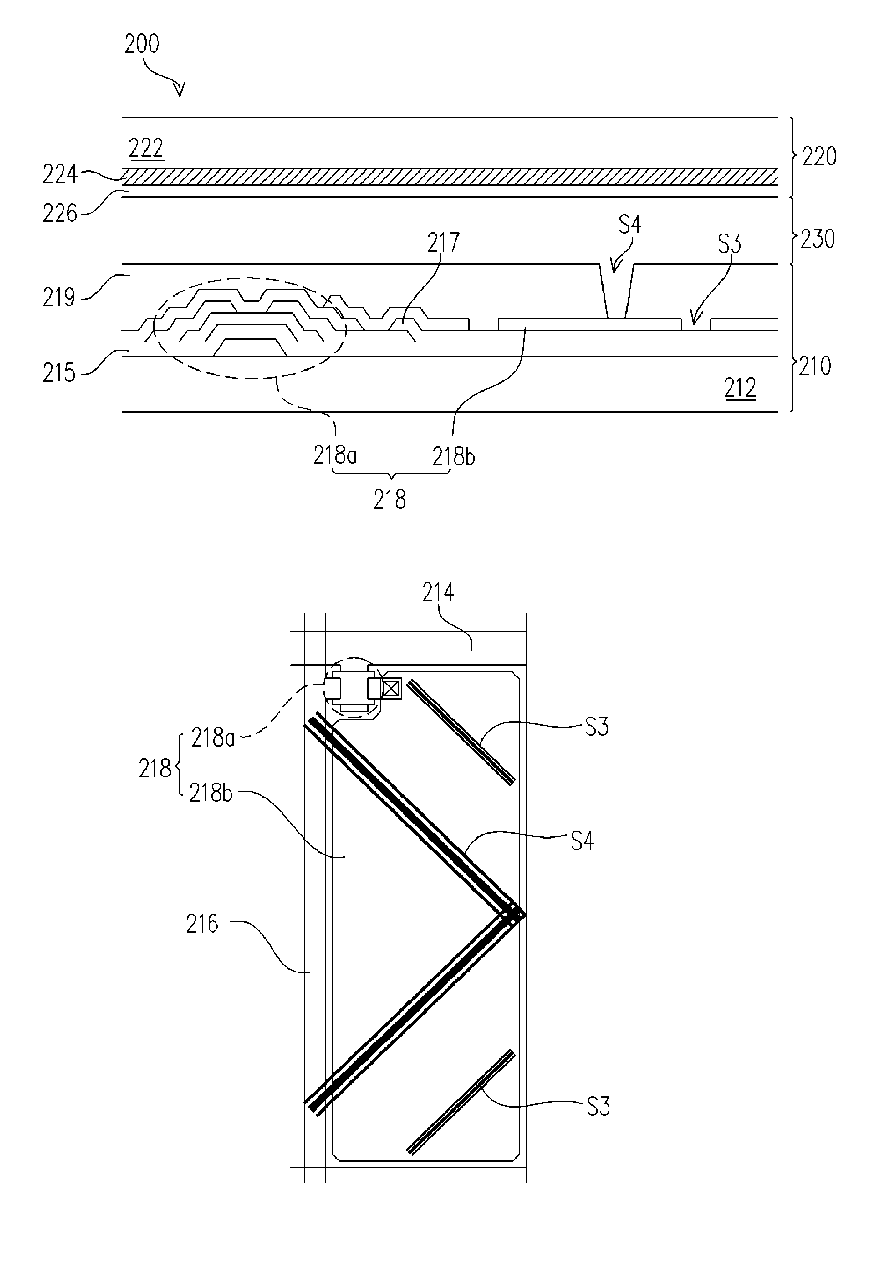
[0038]FIGS. 3 and 3′ are respectively a cross-sectional view and a top view of an MVA-LCD panel according to the first embodiment of the invention. Referring to FIGS. 3 and 3′, an MVA-LCD panel 200 according to the embodiment includes an active matrix substrate 210, an opposite substrate 220 and a liquid crystal layer 230. The liquid crystal layer 230 is disposed between the active matrix substrate 210 and the opposite substrate 220.

[0039] Referring to FIGS. 3 and 3′, the active matrix substrate 210 of the MVA-LCD panel 200 includes a substrate 212, a plurality of scan lines 214, a plurality of data lines216, a plurality of pixel units 218 and a dielectric layer 219. The scan lines 214, the data lines 216, the pixel units 218 and the dielectric layer 219 are all disposed on the substrate 212. The scan lines 214, the data lines 216 are electrically connected with the corresponding pixel units 218. More specifically, the scan lines 214 for example extend along wit...

second embodiment

The Second Embodiment

[0049]FIGS. 5 and 5′ are respectively a cross-sectional view and a top view of an MVA-LCD panel according to the second embodiment of the invention. Referring to FIGS. 5 and 5′, the MVA-LCD panel 200′ of the embodiment is similar to the MVA-LCD panel 200 of the first embodiment except the structure of the pixel unit 218′. Specifically, the pixel unit 218′ illustrated in the second embodiment includes a active device 218a, a pixel electrode 218b and a light shielding layer 218c. As shown in FIGS. 5 and 5′, the light shielding layer 218c is disposed under the second slit S4 of the dielectric layer 219. In an alternative embodiment, the light shielding layer 218c is preferred but not limited to have a width larger than the width of the second slit S4. It should be noted that the employment of the light shielding layer 218c can effectively avoid the light leakage caused by the second slits S4 and further enhance the contrast ratio of the MVA-LCD panel 200′.

[0050] F...

third embodiment

The Third Embodiment

[0053]FIGS. 7 and 7′ are respectively a cross-sectional view and a top view of an MVA-LCD panel according to the third embodiment of the invention. Referring to FIGS. 7 and 7′, the MVA-LCD panel 200″ of the embodiment is similar to the MVA-LCD panel 200′ of the second embodiment except the structure of the pixel unit 218″. The pixel unit 218″ illustrated in the third embodiment includes an active device 218a, a pixel electrode 218b, a the light shielding layer (lower electrode) 218c and an upper electrode 218d. The upper electrode 218d is disposed between the light shielding layer 218c and the second slit S4 of the dielectric layer 219. The upper electrode 218d is electrically connected with the pixel electrode 218b via a contacting window 217b of a passivation layer 217. In an alternative embodiment, the upper electrode 218d is preferred but not limited to have a width larger than the width of the second slit S4. It should be noted that the light shielding layer...


PUM


Abstract

An active matrix substrate is provided. The active matrix substrate includes a substrate, a plurality of scan lines disposed on the substrate, a plurality of data lines disposed on the substrate, a plurality of pixel units disposed on the substrate and a dielectric layer disposed on the substrate. The pixel units are electrically connected with the corresponding scan lines and data lines. Each pixel unit includes an active device and a pixel electrode electrically connected with the active device, such a pixel electrode includes at least a first slit. The dielectric layer covers the first slit, and the dielectric layer includes a plurality of second slits for exposing a part of each of the pixel electrodes.

Description

CROSS-REFERENCE TO RELATED APPLICATION [0001] This application claims the priority benefit of Taiwan application serial no. 94114860, filed on May 09, 2005. All disclosure of the Taiwan application is incorporated herein by reference. BACKGROUND OF THE INVENTION [0002] 1. Field of the Invention [0003] The present invention relates to a liquid crystal display panel, and particularly, to a multi-domain vertical alignment liquid crystal display (MVA-LCD) panel. [0004] 2. Description of Related Art [0005] Nowadays, the thin film transistor liquid crystal display (TFT-LCD) is highly required having the characteristics of high contrast ratio, no gray scale inversion, little color shift, high luminance, high color richness, high color saturation, rapid response and wide viewing angle. The conventional displays which can match the demand for wide viewing angle include twisted nematic (TN) LCDs with wide viewing films, in-plane switching (IPS) LCDs, fringe field switching (FFS) LCDs and mult...

Claims


Application Information

Patent Timeline
IPC IPC(8): G02F1/1343
CPCG02F1/133707G02F2201/128G02F1/1393
Inventor WU, MING-CHOUPAN, HSIN-HUA
Owner AU OPTRONICS CORP
Features
  • Generate Ideas
  • Intellectual Property
  • Life Sciences
  • Materials
  • Tech Scout
  • Unparalleled Data Quality
  • Higher Quality Content
  • 60% Fewer Hallucinations
Learn More