Method and apparatus for low voltage write in a static random access memory

a random access memory and low voltage technology, applied in the field of memory, can solve the problems of affecting bit cell read and write operations, affecting the general design of circuits of almost all, and affecting the type of things that improve the read , to achieve the effect of reducing the write ra

Active Publication Date: 2006-11-09
NXP USA INC
View PDF4 Cites 5 Cited by
  • Summary
  • Abstract
  • Description
  • Claims
  • Application Information

AI Technical Summary

Problems solved by technology

This has created a number of problems in general for circuit designs of almost all types.
In regard to static random access memories (SRAMs) both the bit cell read and write operations have been adversely affected.
What further compounds this problem with SRAMs is that the types of things that improve the read tend to degrade the write.
Similarly, the things that tend to improve the write degrade the read.

Method used


Image

  • Method and apparatus for low voltage write in a static random access memory
  • Method and apparatus for low voltage write in a static random access memory
  • Method and apparatus for low voltage write in a static random access memory

Examples


Embodiment Construction

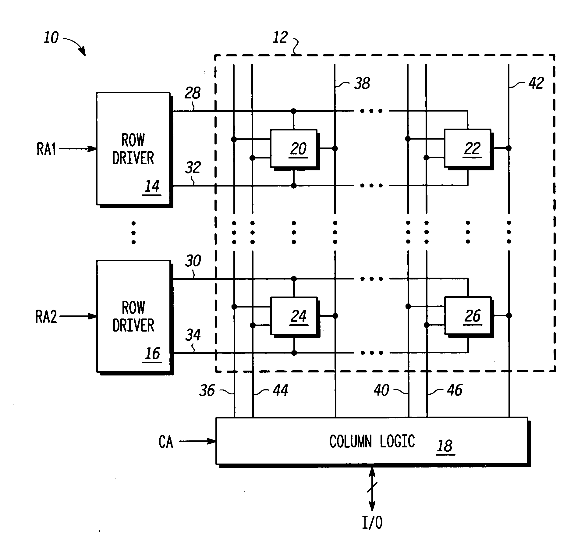
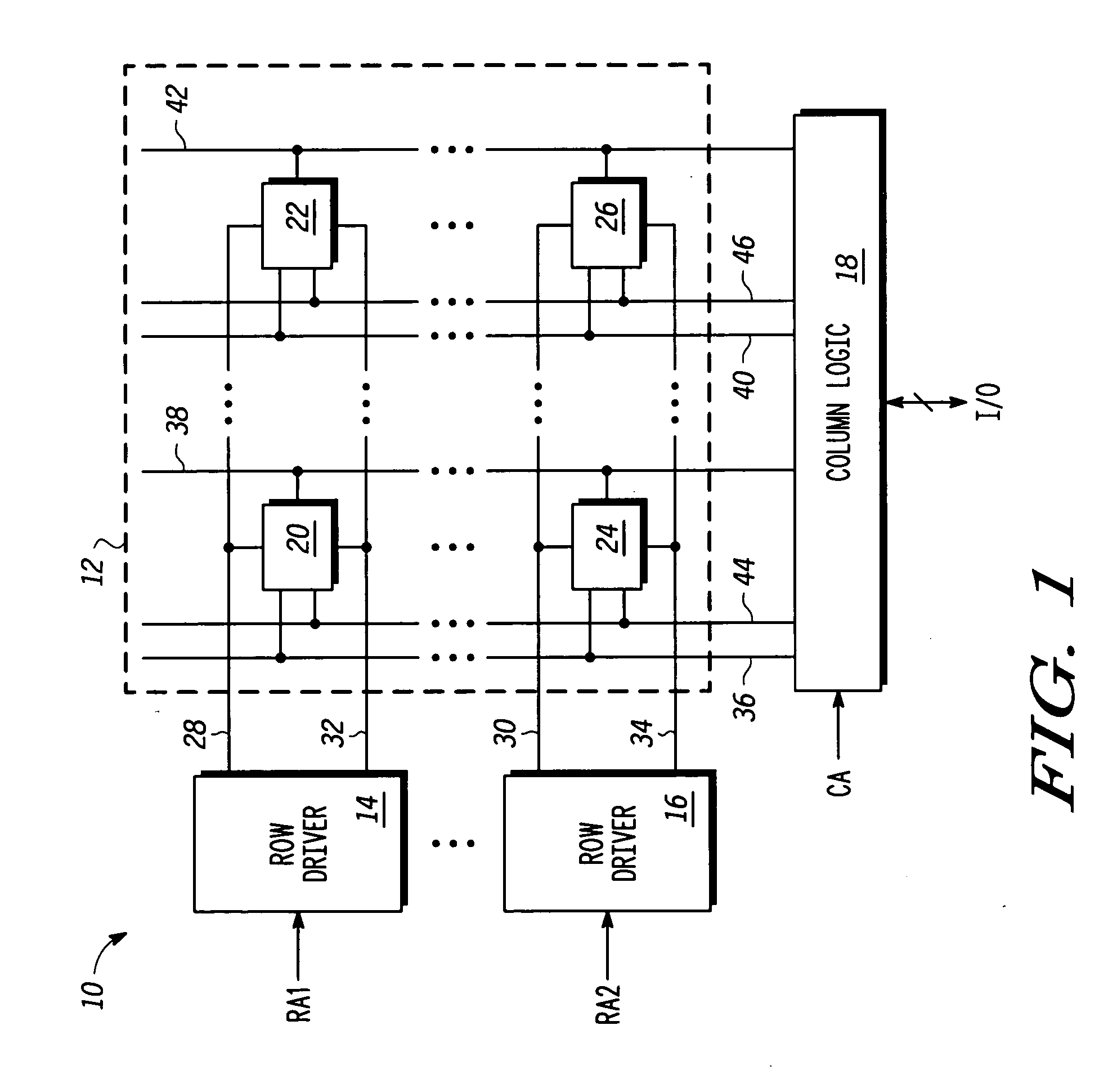
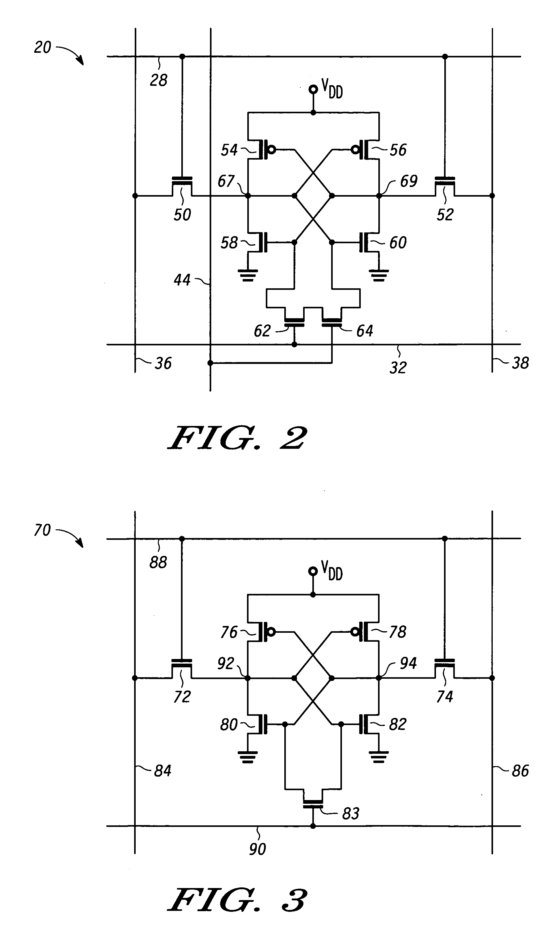
[0007] In one aspect, a static random access memory (SRAM) has an array with memory cells with cross coupled inverters, which is typical for SRAMs. In order to improve the reliability of the write operation, the outputs of the inverters are coupled together by an equalization transistor during the beginning portion of the write operation. There is a time during the write in which both write data is applied to the memory cells and the outputs of the inverters are being shorted. After both of these have occurred together, the equalization transistor is made non-conductive so that the inverters can assume the logic state being written. This is achieved with write data that is provided at the full rail of the power supply voltages in order to obtain reliable write. This improves the write reliability while allowing for improving the read operation as well. This is better understood with reference to the FIGs. and the following description.

[0008] Shown in FIG. 1 is a memory 10 comprisin...


PUM


Abstract

An integrated circuit memory includes a plurality of memory cells, where each of the plurality of memory cells comprises a first storage node and a second storage node. Each of the plurality of memory cells comprises a transistor coupled between the first and second storage nodes and responsive to an equalization signal. An equalization control circuit provides the equalization signal to selected memory cells of the plurality of memory cells. The equalization control circuit is for equalizing a voltage between the first and second storage nodes to enable to a write operation of the selected memory cells. During the write operation a data signal is provided to a first bit line that swings between a logic high voltage equal to a power supply voltage and a logic low voltage equal to ground potential. The transistor and the equalization control circuit enables reliable memory operation at low power supply voltages.

Description

FIELD OF THE INVENTION [0001] This invention relates generally to memories, and more particularly to writing static random access memories in a low voltage power supply environment. RELATED ART [0002] Integrated circuits are using lower and lower power supply voltages in order to reduce current leakage. This has created a number of problems in general for circuit designs of almost all types. In regard to static random access memories (SRAMs) both the bit cell read and write operations have been adversely affected. What further compounds this problem with SRAMs is that the types of things that improve the read tend to degrade the write. Similarly, the things that tend to improve the write degrade the read. Thus, there is a need to improve one without degrading the other.BRIEF DESCRIPTION OF THE DRAWINGS [0003] The present invention is illustrated by way of example, and not by way of limitation, in the figures of the accompanying drawings and in which like reference numerals refer to ...

Claims


Application Information

Patent Timeline
Patent Type & Authority Applications(United States)
IPC IPC(8): G11C11/00
CPCG11C11/419
Inventor RAMARAJU, RAVINDRARAJKENKARE, PRASHANT U.PELLEY, PERRY H.
Owner NXP USA INC
Why Eureka
Try Eureka