Integrated semiconductor memory device for synchronizing a signal with a clock signal

a technology of integrated semiconductor memory and clock signal, which is applied in the direction of information storage, static storage, digital storage, etc., can solve the problems of inability to reset intermediately, inability to align control signals, and inability to achieve stable adjustment of clock signals, etc., and achieve the effect of great reliability

Inactive Publication Date: 2006-11-09
POLARIS INNOVATIONS
View PDF3 Cites 37 Cited by
  • Summary
  • Abstract
  • Description
  • Claims
  • Application Information

AI Technical Summary

Benefits of technology

[0021] The present invention provides an integrated semiconductor memory devi...

Problems solved by technology

However, this is not possible because the time-shifted internal read command signal OUT is generated after the latency counter circuit 30 is actuated by the internal read command signal PAR.
However, misaligned control signals remain stable until the next reset of the DLL circuit.
Intermediate resets are not possible.
This means that the solution usually applied for graphic DRAMs does not allow a self-adjustment of the control signals iPoint′ and oPoint′.
Further...

Method used


Image

  • Integrated semiconductor memory device for synchronizing a signal with a clock signal
  • Integrated semiconductor memory device for synchronizing a signal with a clock signal
  • Integrated semiconductor memory device for synchronizing a signal with a clock signal

Examples


Embodiment Construction

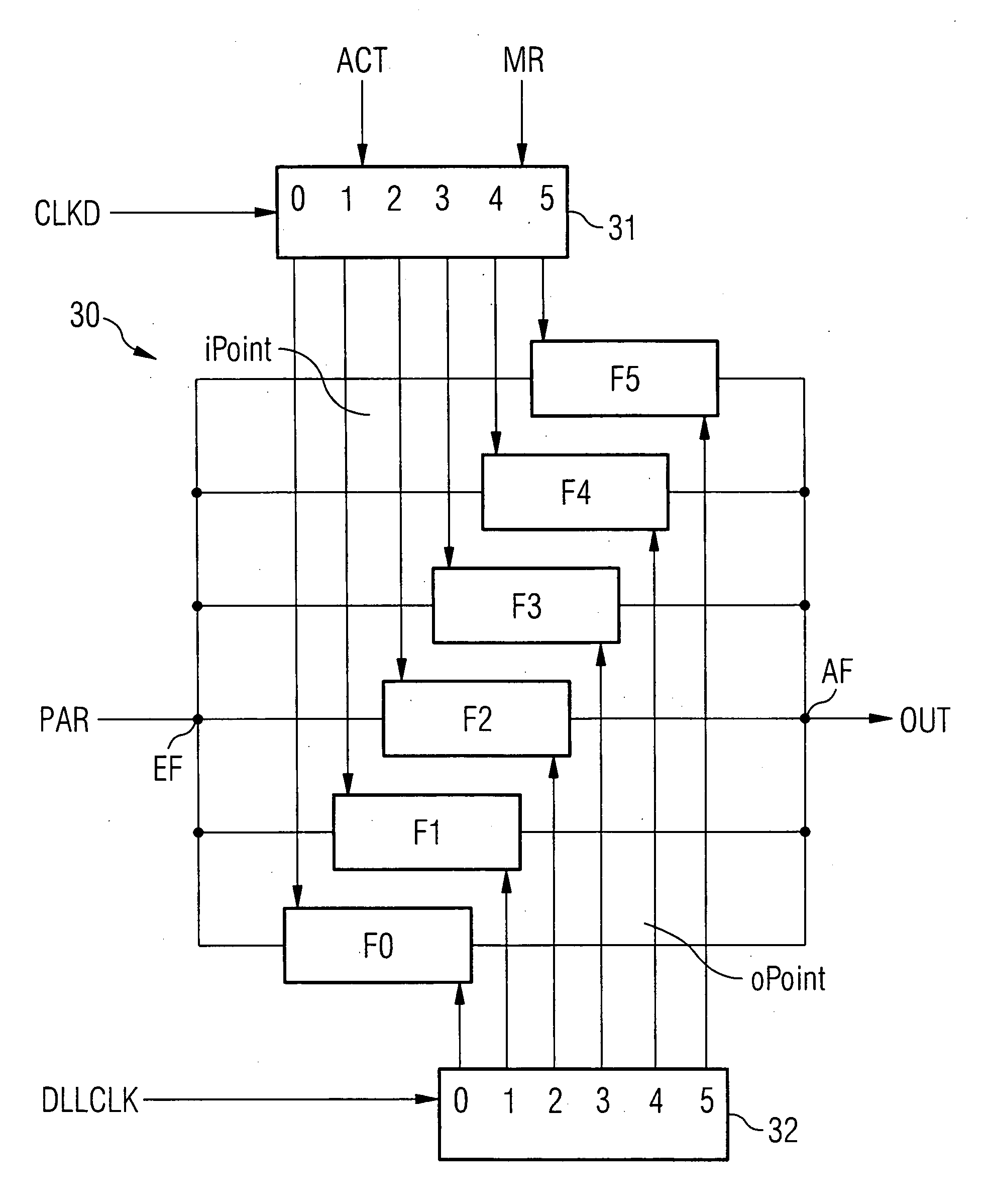
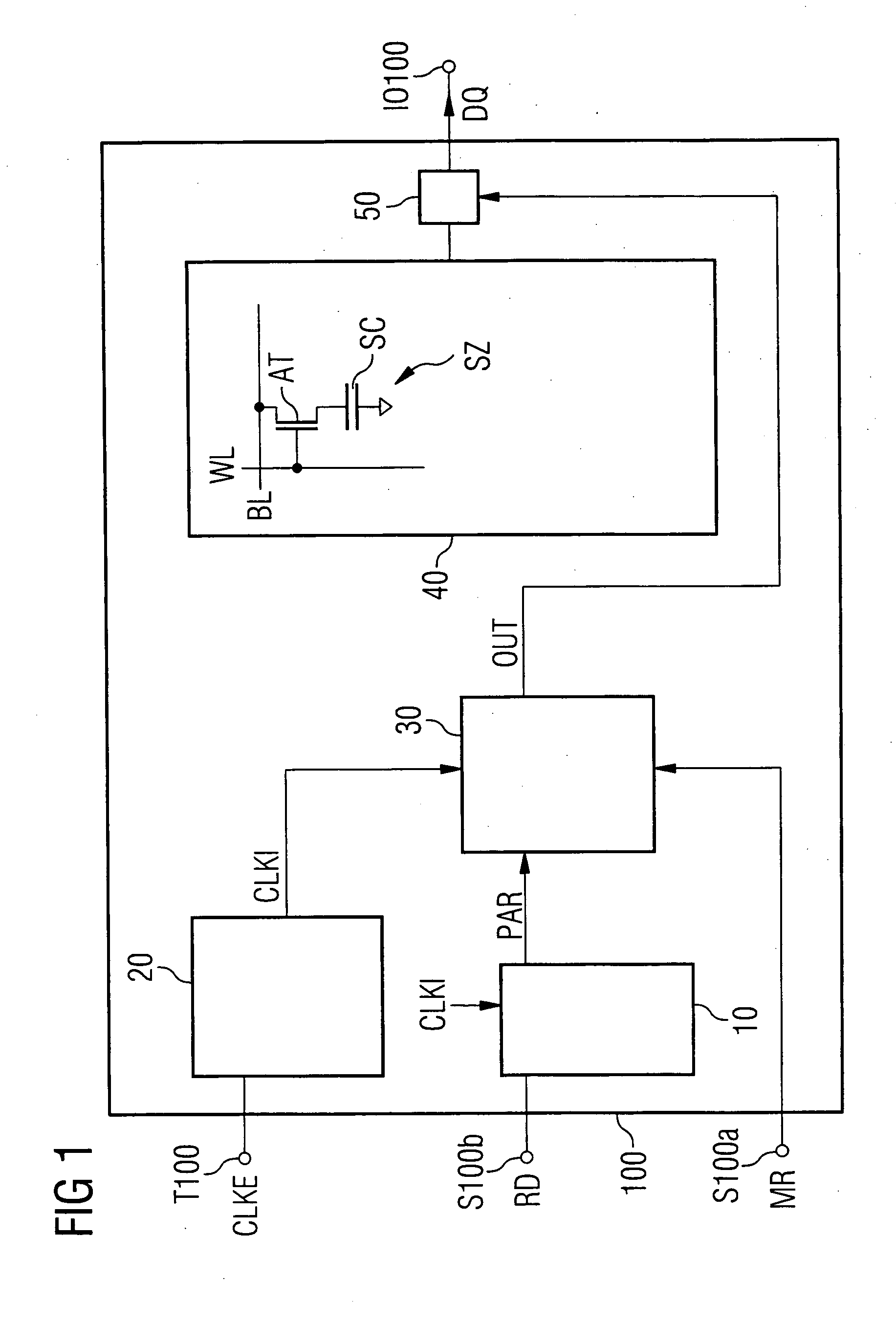
[0065]FIG. 5 shows an integrated semiconductor memory device for synchronizing data items DQ which appear, after a read access, at data terminal IO100 synchronous with a clock cycle of an external clock signal CLKE according to the present invention. An external read command signal RD is applied to a control terminal S100b to indicate a read access to a memory cell inside a memory cell array 40. A memory cell inside the memory cell array is activated and a data item stored therein is transferred to and buffered in an output circuit 50. A control circuit 10 is connected to the control terminal S100b and generates an internal read command signal PAR. The internal read command signal PAR is transmitted to a latency counter circuit 30. Depending on a configuration signal MR which is applied to a control terminal S100a and indicates a CAS latency, it generates a time-shifted internal read command signal OUT. The time-shifted internal read command signal OUT actuates the output circuit 50...


PUM


Abstract

A semiconductor memory includes a control circuit for generating an internal read command signal depending on an externally applied read command signal. A clock generating circuit generates a system clock signal and a time shifted clock signal generated by a DLL circuit. A latency counter circuit comprises a first control circuit for generating a first control signal and a second control circuit for generating a second control signal. The first control signal is used to latch the internal read command signal in one of FIFO-latching cells. The latching is carried out in a system clock domain. The second control signal is used to release a time shifted internal read command signal from one of the FIFO-latching cells in a DLL clock domain. The relationship between first and second control signals determines a CAS latency by which data items appear at a data terminal synchronous with an externally applied clock signal.

Description

FIELD OF THE INVENTION [0001] The invention relates to an integrated semiconductor memory device for synchronizing a signal, such as a data signal, with a clock signal, and a method for the same. BACKGROUND OF THE INVENTION [0002]FIG. 1 shows a semiconductor memory 100 with a memory cell array 40. The memory cell array comprises memory cells which are designed as DRAM (dynamic random access memory) cells, for example. For the sake of simplicity, only one memory cell comprising a storage capacitor SC and a selection transistor AT is illustrated in the memory cell array 40. The control terminal of the selection transistor AT is connected to a wordline WL. The storage capacitor SC is connected to a terminal for application of a reference potential, and is also connected to a bitline BL via the controllable path of the selection transistor. [0003] Read or write accesses are controlled synchronously with an external clock signal CLKE, applied to a clock terminal T100. A clock receiver ci...

Claims


Application Information

Patent Timeline
IPC IPC(8): G11C8/00
CPCG11C7/1066G11C7/1072G11C11/4076G11C7/222G11C8/18G11C7/22G11C8/04
Inventor SZCZYPINSKI, KAZIMIERZ
Owner POLARIS INNOVATIONS
Why Eureka
Try Eureka