Probing system for integrated circuit devices

a technology of integrated circuit devices and probes, which is applied in the direction of transmission, transmission monitoring, instruments, etc., can solve the problems that the overall time accuracy cannot catch up with the increasing high operation speed of integrated circuit devices, and achieve the effect of high operation speed and better overall time accuracy

Inactive Publication Date: 2006-11-09
NATIONAL TSING HUA UNIVERSITY
View PDF10 Cites 40 Cited by
  • Summary
  • Abstract
  • Description
  • Claims
  • Application Information

AI Technical Summary

Benefits of technology

[0007] The objective of the present invention is to provide a probing system for integrated circuit devices, which can provide a better overall time accuracy for the application to the electrical testing of integrated circuit devices with a high operation speed.

Problems solved by technology

The prior art uses a mechanical element, i.e., the tip, to transmit testing data, and therefore the overall time accuracy cannot catch up with the increasing high operation speed of integrated circuit devices.

Method used


Image

  • Probing system for integrated circuit devices
  • Probing system for integrated circuit devices
  • Probing system for integrated circuit devices

Examples


first embodiment

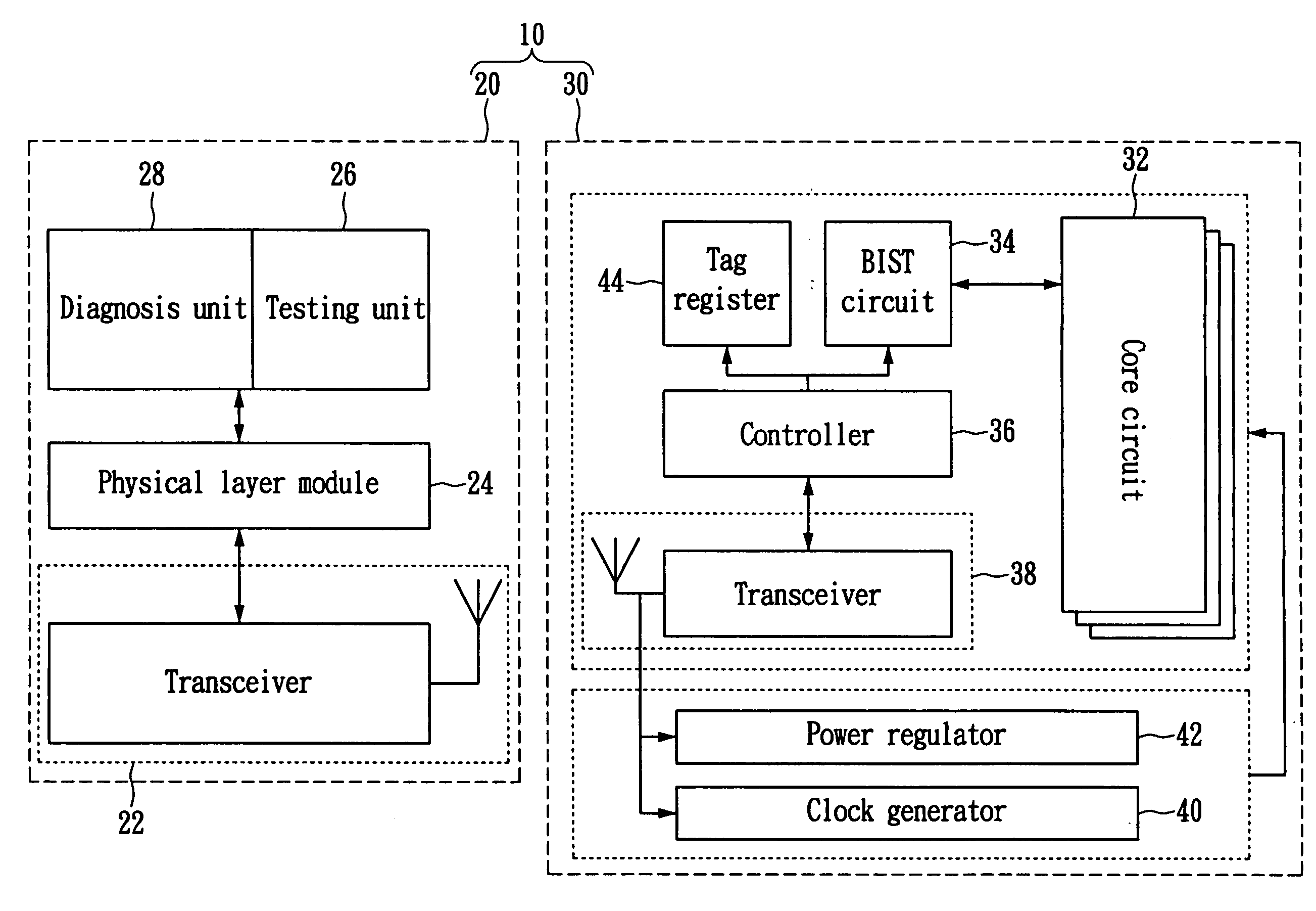
[0015]FIG. 1 illustrates a probing system 10 for integrated circuit devices according to the present invention, in which testing data such as the probing signal and the tested electrical parameter is transmitted between a testing machine 20 and an integrated circuit device 30 in a wireless manner. The testing machine 20 comprises a first transceiving module 22, a physical layer module 24 electrically connected to the first transceiving module 22, a testing unit 26 electrically coupled to the physical layer module 24, and a diagnosis unit 28 electrically coupled to the physical layer module 24. The integrated circuit device 30 such as a system on chip (SOC) comprises a core circuit 32, a built-in self-test (BIST) circuit 34 electrically connected to the core circuit 32, a controller 36 configured to control the operation of the BIST circuit 34, and a second transceiving module 38 configured to exchange testing data with the first transceiving module 22. The first transceiving module ...

second embodiment

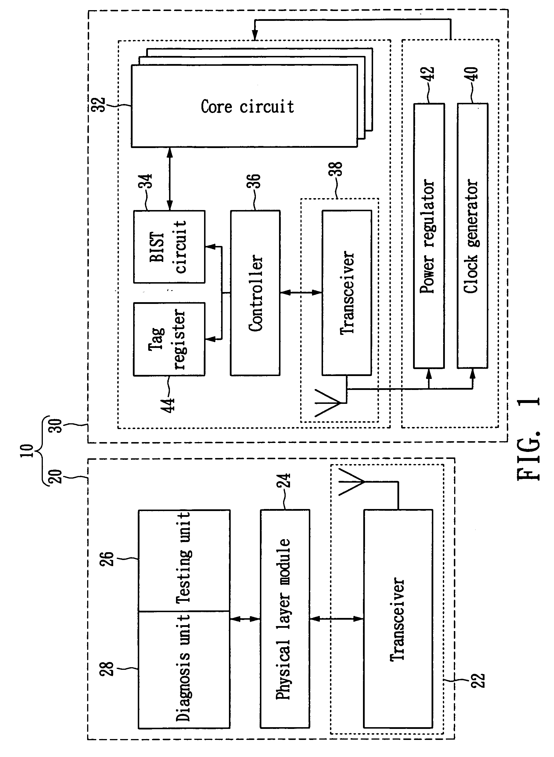
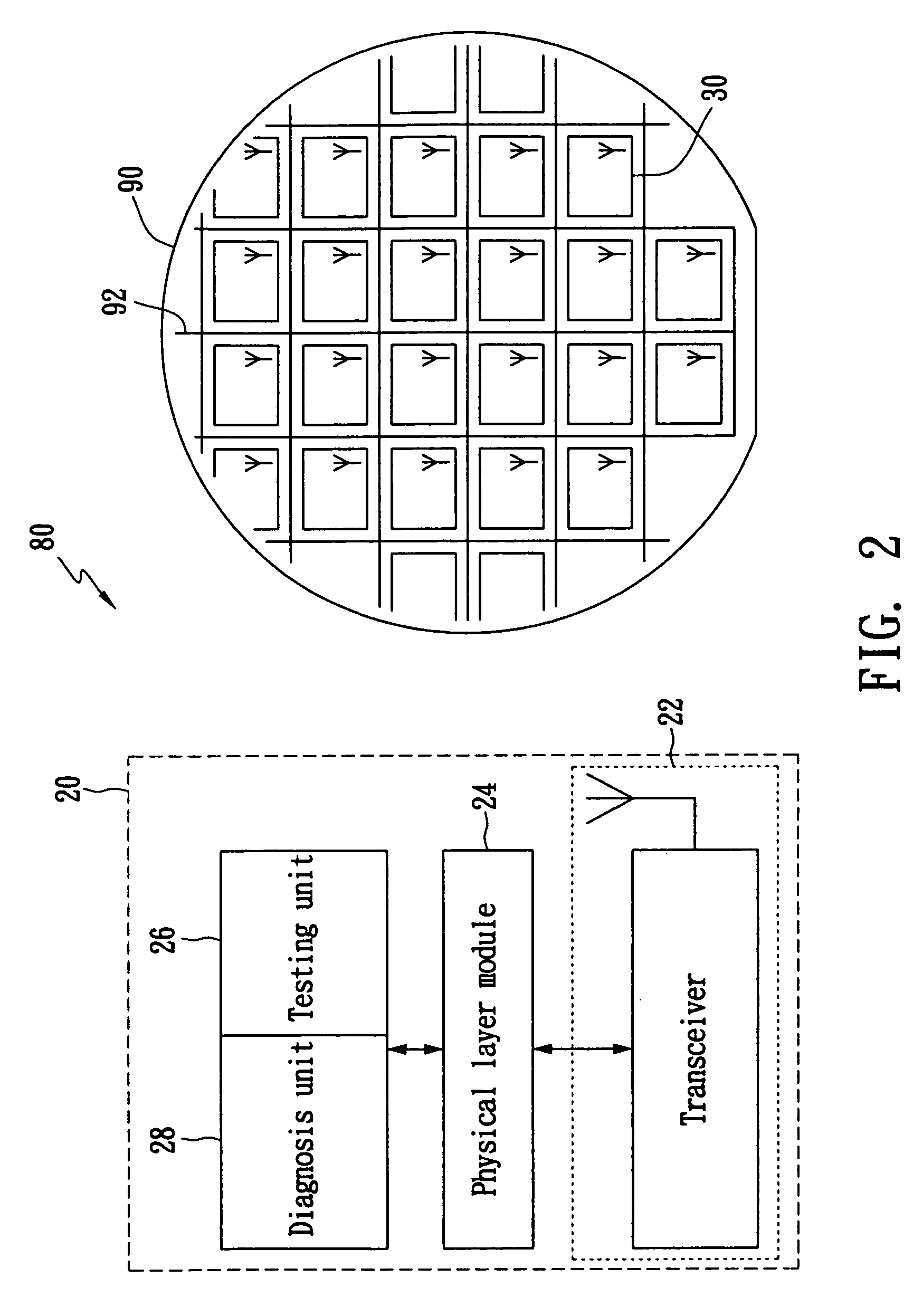
[0017]FIG. 2 illustrates a probing system 80 for integrated circuit devices according to the present invention, which is applied to the electrical testing of a plurality of integrated circuit device 30 on a wafer. Particularly, the probing system 80 is applied to the electrical testing of the integrated circuit device 30 at a wafer level. During the electrical testing process, the testing machine 20 first transmits a radio frequency signal by the first transceiving module 22 and the second transceiving module 32 receives the radio frequency signal to drive the power regulator 42 to generate the operation power for the integrated circuit device 30. The testing unit 26 of the testing machine 20 sets an identification to each integrated circuit device 30 by the first transceiving module 22, and each integrated circuit device 30 stores its own identification in the tag register 44. Subsequently, the testing unit 26 transmits an activation instruction to the second transceiving module 32...

third embodiment

[0018]FIG. 3 illustrates a probing system 70 for integrated circuit devices according to the present invention, which is applied to the final testing of an encapsulated die 72. As shown in FIG. 2, the wafer 90 is cut into a plurality of integrated circuit device 30, and those which meet electrical properties specifications are selected to perform the subsequent packaging process, while others that do not meet the specifications are discarded. The testing unit 26 transmits an activation instruction to the second transceiving module 32 to activate the BIST circuit 34 to perform the electrical testing of the core circuit 32, and the diagnosis unit 28 then accumulates testing data transmitted from each integrated circuit device 30 after the electrical testing is completed and checks if the integrated circuit device 30 meets the specifications of the electrical properties and analyzes the failure cause of any failed devices.


PUM


Abstract

The present invention discloses a probing system for integrated circuit devices, which transmits testing data between an automatic test equipment (ATE) and an integrated circuit device. The ATE includes a first transceiving module, and the integrated circuit device includes a core circuit, a built-in self-test (BIST) circuit electrically connected to the core circuit, a controller configured to control the operation of the BIST circuit, and a second transceiving module configured to exchange testing data with the first transceiving module. Preferably, the integrated circuit device further includes a clock generator and a power regulator electrically connected to the second transceiving module, wherein the ATE transmits a radio frequency signal via the first transceiving module, and the second transceiving module receives the radio frequency signal to drive the power regulator to generate power for the integrated circuit device to initiate the BIST circuit.

Description

RELATED U.S. APPLICATIONS [0001] Not applicable. STATEMENT REGARDING FEDERALLY SPONSORED RESEARCH OR DEVELOPMENT [0002] Not applicable. REFERENCE TO MICROFICHE APPENDIX [0003] Not applicable. FIELD OF THE INVENTION [0004] The present invention relates to a probing system for integrated circuit devices, and more particularly, to a probing system for integrated circuit devices in which testing data is transmitted in a wireless manner. BACKGROUND OF THE INVENTION [0005] Generally speaking, before an integrated circuit device is packaged, a testing process is performed to check the electrical properties of the integrated circuit device on a wafer. The integrated circuit devices that meet the specifications of the electrical properties are selected for the subsequent packaging process, while others that do not meet the specifications are discarded to cut the packaging cost. [0006] The conventional automatic test equipment (ATE) uses probe tips on a probe card to contact signal pads on a ...

Claims


Application Information

Patent Timeline
Patent Type & Authority Applications(United States)
IPC IPC(8): H04B17/00
CPCG01R31/3025H04B17/0085G01R31/303
Inventor WU, CHENG-WENHUANG, CHIH-TSUNHSING, YU-TSAO
Owner NATIONAL TSING HUA UNIVERSITY
Why Eureka
Try Eureka