Light emitting diode light source model

Inactive Publication Date: 2006-11-16
QUASAR OPTOELECTRONICS INC TW
View PDF3 Cites 12 Cited by
  • Summary
  • Abstract
  • Description
  • Claims
  • Application Information

AI Technical Summary

Benefits of technology

[0009] The main objective of the present invention is to provide an LED light source model suitable for flat

Problems solved by technology

However, the heat from the LED element in operation mode effects the reliability of the LED element.
However, those many elements occupy too much space an

Method used


Image

  • Light emitting diode light source model
  • Light emitting diode light source model
  • Light emitting diode light source model

Examples


first embodiment

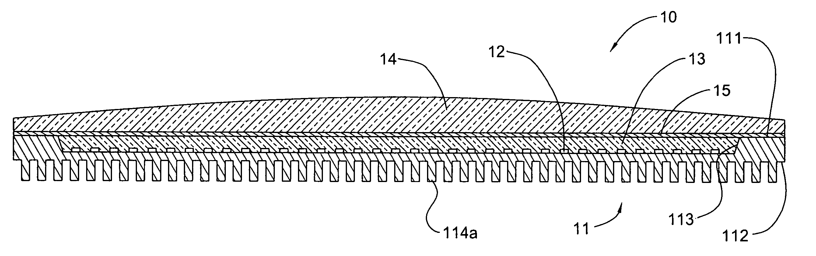
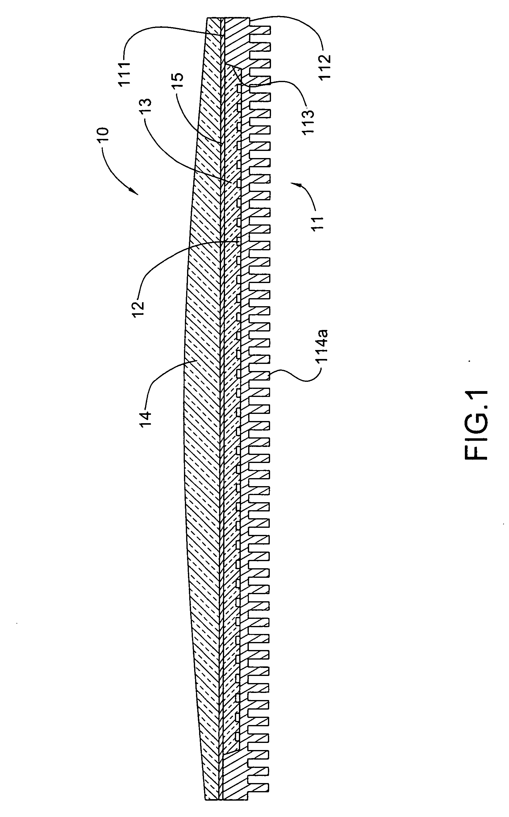
[0018] With reference to FIG. 1, an LED light source model (10) in accordance with the present invention has a substrate (11) with high thermal conductivity, at least one bare LED chip (12), a transparent protection layer (13), and an optical light collecting element (14).

[0019] Since the substrate (11) has high thermal conductivity, the substrate (11) can be made of metal material (such as aluminum, copper, alloy or the like etc.) or nonmetal (such as a ceramics or the like). The substrate (11) has a top face (111), a bottom face (112), at least one chip cup (113) is defined on the top face (111) and a plurality of fins (114a) or recesses are formed on or defined in the bottom face (112). The chip cup (113) is able to be defined as a cone shape. The fins (114a) or the recesses are formed to increase the heat dissipation area of the substrate (11). The fins (114a) are formed as straight shapes and arranged parallel to each other on the bottom face. Therefore, the substrate (11) is a...

second embodiment

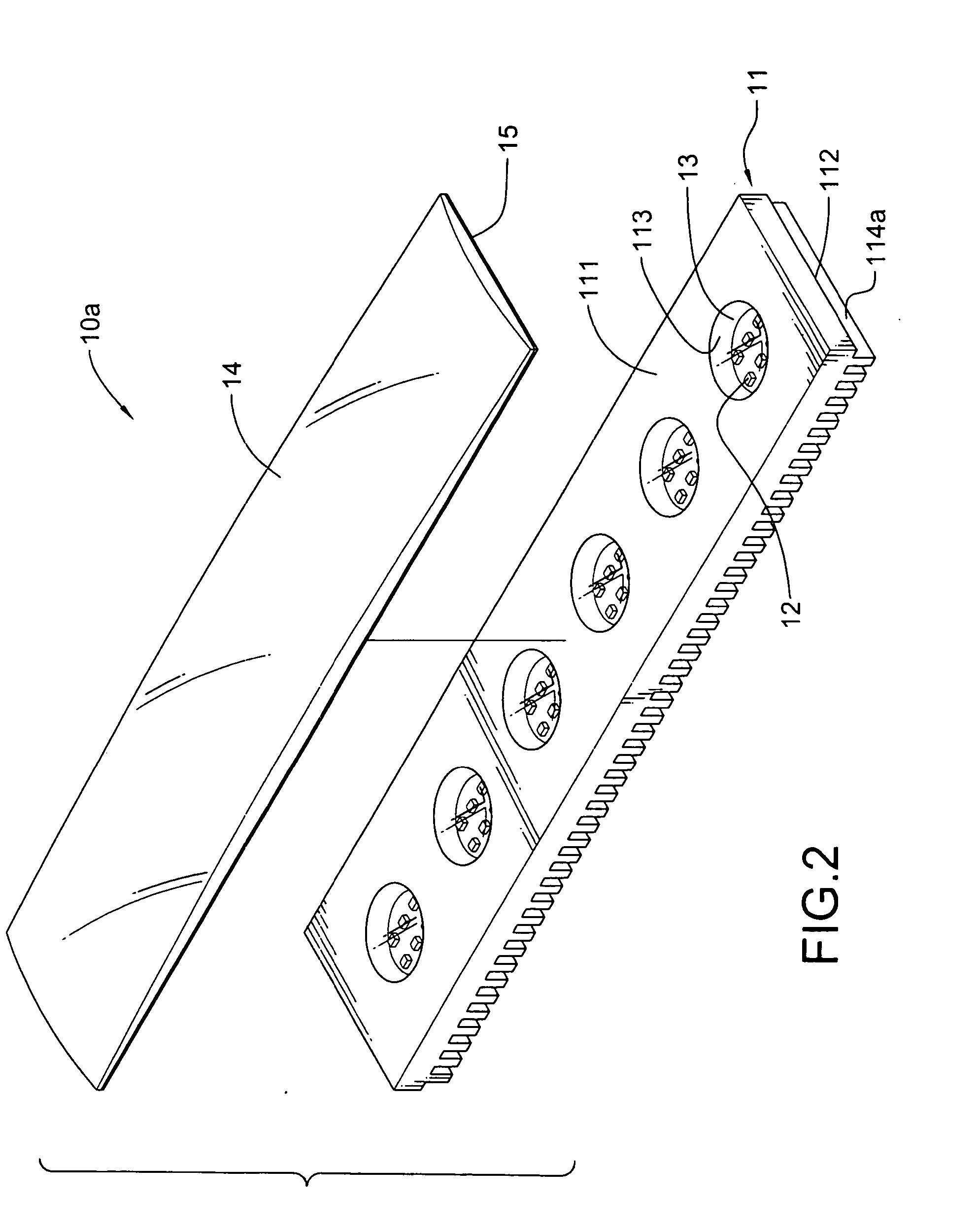
[0022] With reference to FIGS. 2 and 3, an LED light source model (10a) in accordance with the present invention has a plurality of chip cups (113) defined in the top face (111) of the substrate (11). A plurality of bare LED chips (12) are mounted in each chip cup (113).

[0023] With reference to FIGS. 4 and 5, third and fourth embodiments of an LED light source model (10b, 10c) have different substrates (11b, 11c). The fins (114b) of the substrate (11b) in FIG. 4 are formed as wave shapes and are also arranged parallel to each other on the bottom face of the substrate. The fins (114c) of the substrate (11c) in FIG. 5 are formed as saw tooth shapes and are also arranged parallel on the bottom face of the substrate. In addition, the plurality of fins also can be formed as a grid.

[0024] In FIG. 5, the plurality of chip cups (113) are defined in the top face (111c) of the substrate (11c) and arranged in a matrix.

[0025] Since the substrate is flat and has high thermal conductivity, heat...


PUM


Abstract

An LED light source model has a substrate, at least one bare LED chip, a transparent layer and an optical light collecting element. The substrate has a top face, a bottom face and at least one chip cup defined on the top face. The at least one LED chip is mounted in the at least one chip cup. The transparent layer is formed on the top face to seal the at least one chip cup. The optical light collecting element is mounted on the top face to collect the light from each chip cup to increase the light intensity. A plurality of fins or recesses are formed or defined on the bottom face to increase a heat dissipation area. When each bare LED chip is in operation mode, heat from the bare LED chip will be conducted to the bottom face and then dissipate to the ambient air quickly.

Description

BACKGROUND OF THE INVENTION [0001] 1. Field of the Invention [0002] The present invention relates to a light emitting diode light (LED) source model, and more particularly to a light emitting diode light source model having a high light intensity, simple structure and high heat dissipation etc. capabilities. [0003] 2. Description of Related Art [0004] The light emitting diode (LED) element is widely used to be a light source of the lamps or illumination devices since the LED element has low power consumption and high enough light intensity. However, the heat from the LED element in operation mode effects the reliability of the LED element. Therefore, many companies or factories in this technology field make efforts in finding or inventing some solutions to decrease the heat influence and also devote research to increase light intensity of the LED element. [0005] With reference to FIG. 6, an LED type bulb (50) having good heat dissipation capability has a casing (51) with a top openi...

Claims


Application Information

Patent Timeline
IPC IPC(8): H01L33/00F21V17/10H01L33/48H01L33/56H01L33/58H01L33/64
CPCF21K9/00F21S2/005F21V29/004F21Y2103/003F21V29/89H01L33/642F21Y2101/02F21V29/763F21Y2105/001F21V29/503F21V31/005F21Y2103/10F21Y2105/10F21Y2115/10
Inventor SUN, TSENG-BAOLEE, KO-HSINXU, YONG-YUAN
Owner QUASAR OPTOELECTRONICS INC TW
Why Eureka
Try Eureka