Thermal processing unit

a technology of thermal processing unit and heat exchanger, which is applied in the direction of muffle furnace, lighting and heating apparatus, furnace, etc., can solve the problems of large thermal capacity inability to meet the recent request of enhancing the throughput of semiconductor manufacturing unit, and inability to meet the recent request of enhancing the throughput of conventional thermal processing unit, etc. the uneven heating of an object to be processed such as a silicon wafer is improved, the effect of rapid cooling

Inactive Publication Date: 2006-11-16
TOKYO ELECTRON LTD
View PDF10 Cites 9 Cited by
  • Summary
  • Abstract
  • Description
  • Claims
  • Application Information

AI Technical Summary

Benefits of technology

[0020] An object of the present invention is to provide a thermal processing unit suitable for rapid heating and rapid cooling in which unevenness in heating an object to be processed such as a silicon wafer is improved.
[0021] Another object of the present invention is to achieve a thermal processing unit and a thermal processing method using the thermal processing unit wherein temperature control is easy and wherein particle generation is effectively prevented.
[0023] According to the invention, since the reaction container consists of a single tube and has a smaller thermal capacity, rapid heating and rapid cooling can be achieved. In addition, since a temperature at the gas-discharging-pipe connecting portion is controlled by the first temperature controlling unit, particle generation at the gas-discharging-pipe connecting portion can be effectively prevented.

Problems solved by technology

However, in the conventional thermal processing unit, since the reaction container has the double-tube structure, the thermal capacity thereof is large.
Thus, the conventional thermal processing unit is not suitable for rapid heating and rapid cooling.
Thus, the conventional thermal processing unit can not satisfy the recent request of enhancing the throughput of a semiconductor manufacturing unit.

Method used


Image

  • Thermal processing unit
  • Thermal processing unit
  • Thermal processing unit

Examples


first embodiment

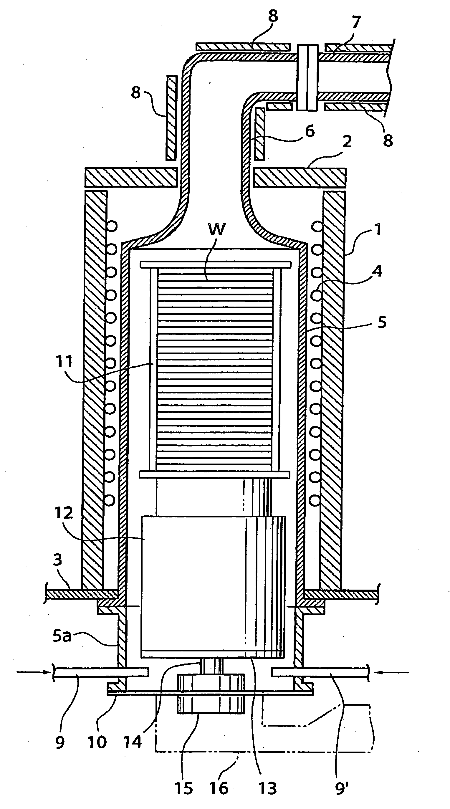
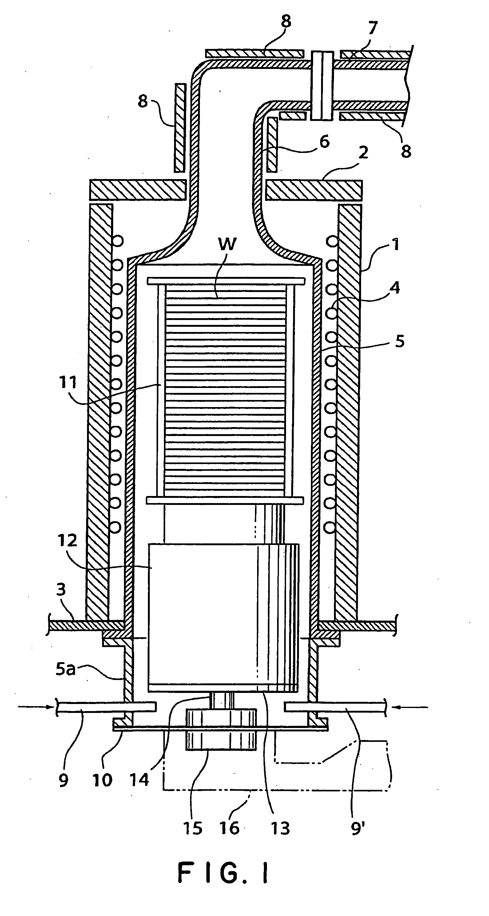
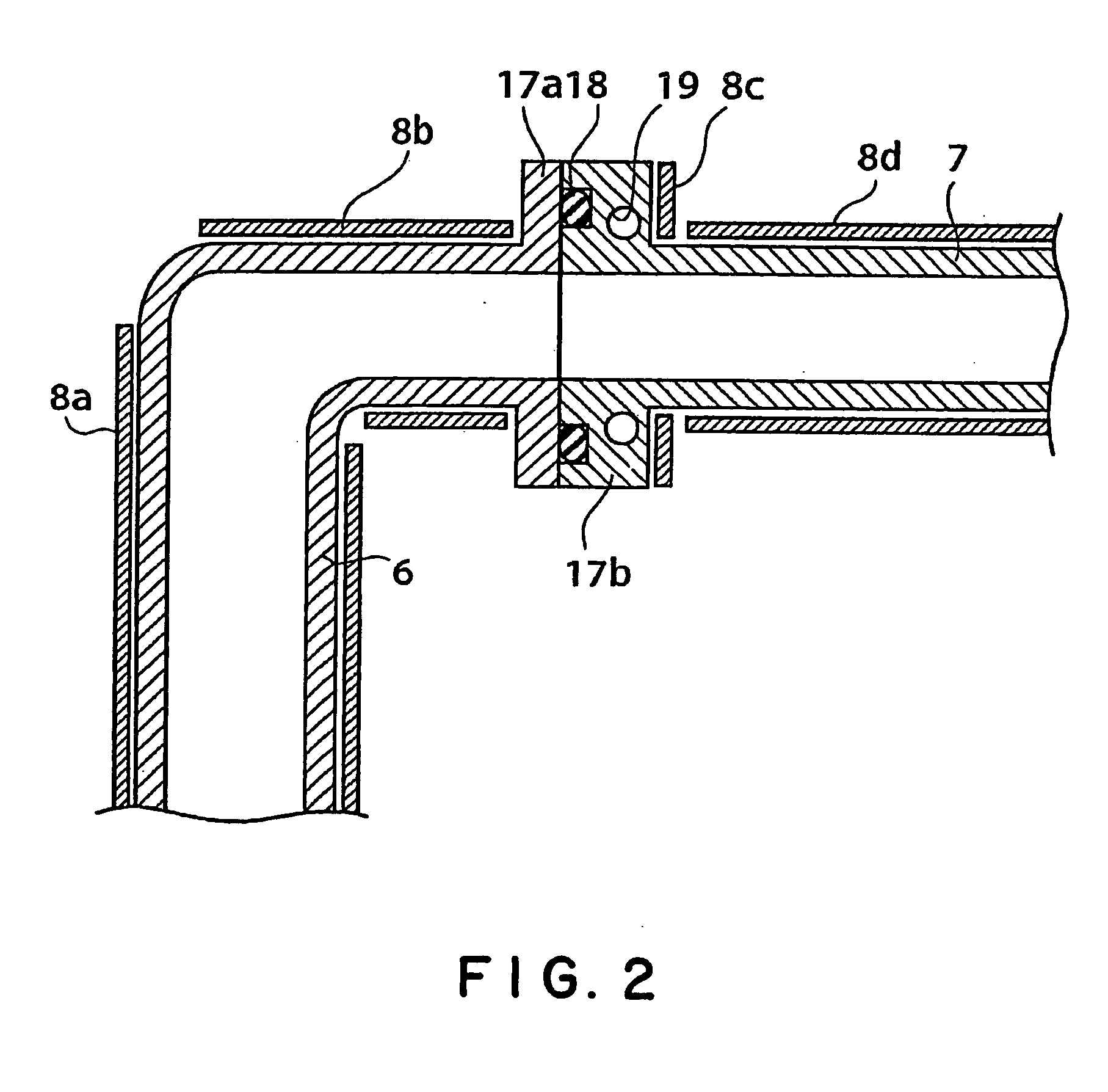
[0045]FIG. 1 is a schematic sectional view showing a thermal processing unit according to a first embodiment of the present invention. The thermal processing unit of the embodiment comprises: a furnace body 1; a process tube 5 of a single-tube structure as a reaction container arranged in the furnace body 1; a gas-discharging-pipe connecting portion 6 extended from the process tube 5; and a gas-discharging pipe 7 closely connected to an end portion of the gas-discharging-pipe connecting portion 6.

[0046] In the thermal processing unit of the embodiment, an upper end of the furnace body 1 has an opening. The opening is covered with a furnace-body lid 2. A central portion of the furnace-body lid 2 is provided with an opening. On the other hand, an upper end of the process tube 5 protrudes to form the gas-discharging-pipe connecting portion 6. Thus, after the process tube 5 is arranged in the furnace body 1, the gas-discharging-pipe connecting portion 6 penetrates the opening of the fu...

second embodiment

[0069] Next, a second embodiment according to the invention is explained. In the second embodiment, arrangements of the heating unit for the reaction container and the temperature controlling units are optimized, uniformity of thermal processing temperature within the surface of a substrate such as a wafer is improved, and generation of defect of the substrate caused by ununiform heating is prevented.

[0070] The thermal processing unit of the second embodiment is shown in FIG. 3. In FIG. 3, the same elements as in FIG. 1 are accompanied with the same numeral references, and the explanation thereof is omitted.

[0071] With reference to FIG. 3, the gas-discharging-pipe connecting portion 6 is formed upward from an upper portion of the process tube 5 by reducing the diameter of the process tube 5. A spiral heater 23 is arranged at a cervical portion of the gas-discharging-pipe connecting portion 6, that is, a portion represented by a numeral reference 25 in FIG. 3. Terminals 24 of the s...

example

[0091] Hereinafter, a specific example of the invention is explained.

[0092] A process tube as shown in FIG. 1 was made of quartz glass.

[0093] 100 silicon wafers were mounted on a wafer boat made of quartz glass in an alignment, and a silicon nitride film having a thickness of 70 nm was deposited on a surface of each silicon wafer at a reaction temperature of 700° C. by using the process tube and by using a silane-base gas as a reaction gas and an ammonium gas. The gas-discharging-pipe connecting portion 6 was heated to 700° C. by means of a carbon wire heater.

[0094] As a comparison, a silicon nitride film was formed under the same conditions, by using a double-tube type of process tube as shown in FIG. 4.

[0095] As a result, in the example of the invention, it took 200 minutes to complete the steps of from preliminary heating to taking-out the silicon wafers. On the other hand, according to the comparison, it took 230 minutes.

[0096] In addition, in both cases, particle contamina...


PUM

PropertyMeasurementUnit
angleaaaaaaaaaa
temperatureaaaaaaaaaa

Abstract

The present invention is a thermal processing unit including: a heating-furnace body whose upper end has an opening; a heating unit provided on an inside wall of the heating-furnace body; a reaction container consisting of a single tube contained in the heating-furnace body; a gas-discharging-pipe connecting portion formed at an upper portion of the reaction container; and a first temperature controlling unit provided around the gas-discharging-pipe connecting portion.

Description

FIELD OF THE INVENTION [0001] The present invention relates to a thermal processing unit and a thermal processing method which are suitable for a thermal process to an object to be processed such as a semiconductor wafer. DESCRIPTION OF THE RELATED ART [0002] Conventionally, in a semiconductor manufacturing process, there is a step of depositing a thin film or an oxide film onto a surface of a semiconductor wafer as an object to be processed, or a step of conducting a diffusion of impurities onto the surface. For these steps, a thermal processing unit such as a CVD unit, an oxide-film forming unit or a diffusion unit has been used. [0003] In such a thermal processing unit, a plurality of wafers, which are objects to be processed, are placed on a holding tool called a wafer boat in a vertical arrangement, and then loaded in a reaction container called a process tube that has been heated to a high temperature. Then, a reaction gas is introduced into the reaction container, so that a t...

Claims


Application Information

Patent Timeline
Patent Type & Authority Applications(United States)
IPC IPC(8): H01L21/31C23C16/44C23C16/455H01L21/00H01L21/205H01L21/22
CPCH01L21/67109H01L21/67098H01L21/67248C23C16/46
Inventor SAITO, TAKANORIMAKIYA, TOSHIYUKIOSANAI, HISAEITAKIZAWA, TSUYOSHISHIMAZU, TOMOHISAHASEBE, KAZUHIDEYAMAMOTO, HIROYUKISAITO, YUKIMASAYAMAGA, KENICHI
Owner TOKYO ELECTRON LTD
Why Eureka
Try Eureka