Semiconductor device and its manufacturing method

a technology of semiconductor devices and manufacturing methods, applied in the direction of semiconductor/solid-state device details, instruments, coatings, etc., can solve the problem of no conventional technical documen

Inactive Publication Date: 2006-11-23
HITACHI LTD
View PDF8 Cites 47 Cited by
  • Summary
  • Abstract
  • Description
  • Claims
  • Application Information

AI Technical Summary

Problems solved by technology

However, as illustratively shown in [Document 1] to [Document 4], there is no conventional technical document which studies an extension of a communication distance by thinning a substrate.

Method used


Image

  • Semiconductor device and its manufacturing method
  • Semiconductor device and its manufacturing method
  • Semiconductor device and its manufacturing method

Examples


Embodiment Construction

[0026] An issue of reducing a product manufacture unit cost exists in wireless IC chips to be used for RFID tags or the like which chips are required to be disposable because wireless IC chips circulate in a massive scale and require a very high collection cost. The issue of reducing a manufacture unit cost can be solved by improving mass productivity by reducing a chip size and increasing the number of chips (RFID tags) capable of being cut from a wafer.

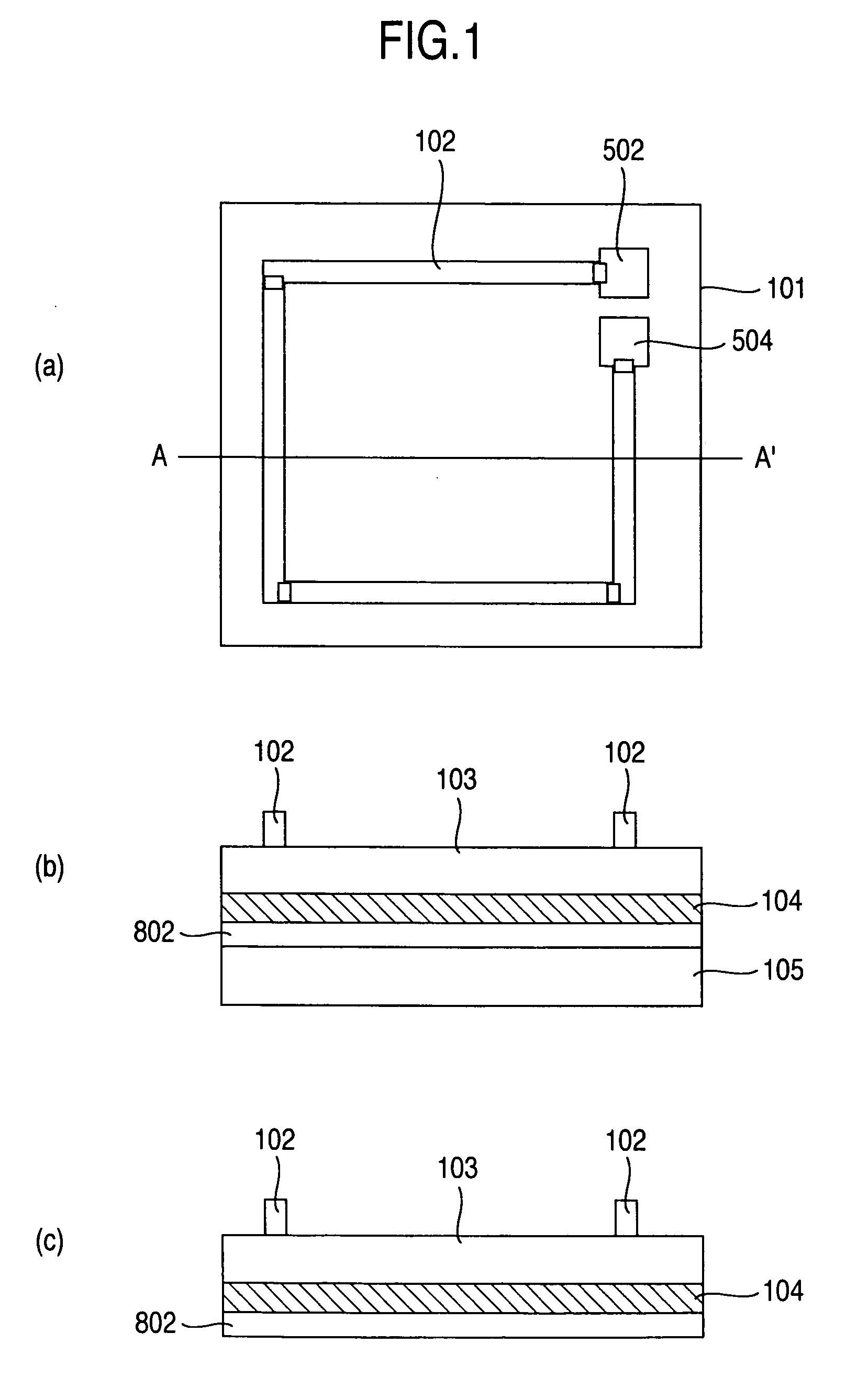
[0027] An antenna on chip can be formed by semiconductor processes of manufacturing a wireless IC chip. As compared with a wireless IC chip having an external antenna, the advantages are considerable in terms of reduction in a manufacture unit cost because it is unnecessary to use components for connecting an antenna to terminals and an antenna connection process.

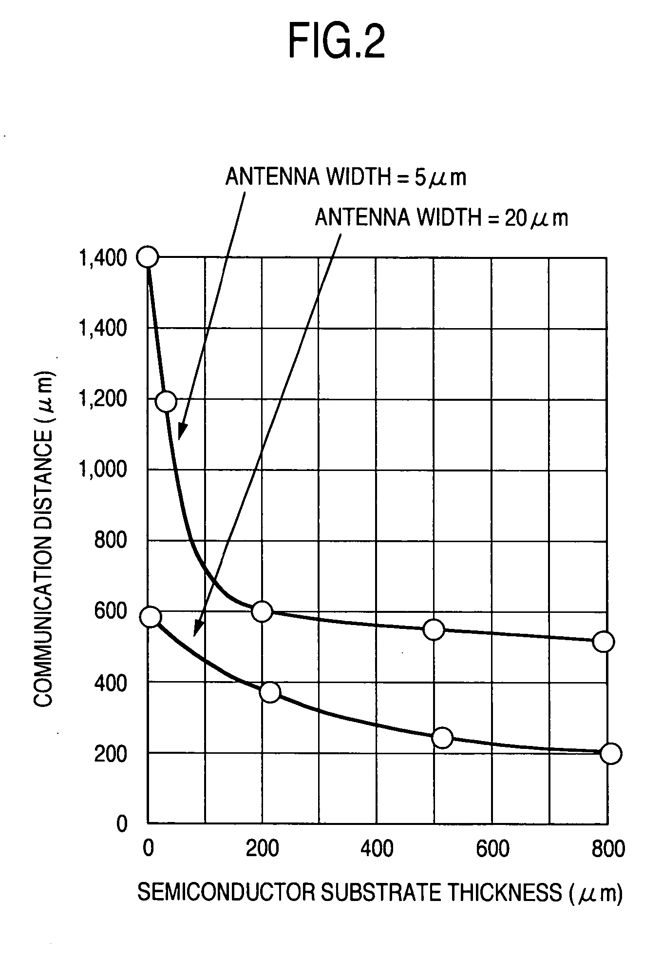
[0028] If an antenna is simply formed on a chip and if only conventionally known design parameters such as an antenna size, an antenna width, an antenna resistance value ...


PUM

PropertyMeasurementUnit
thicknessaaaaaaaaaa
thicknessaaaaaaaaaa
widthaaaaaaaaaa

Abstract

An issue of reducing a product manufacture unit cost exists in wireless IC chips which are required to be disposable because the wireless IC chips circulate in a massive scale and require a very high collection cost. It is possible to increase the communication distance of a wireless IC chip with an on-chip antenna simply contrived for reduction of the production unit cost by increasing the size of the antenna mounted on a wireless IC chip or by increasing the output power of a reader as in a conventional way. However, because of the circumstances of the applications used and the read accuracy of the reader, the antenna cannot be mounted on a very small chip in an in-chip antenna form. When an AC magnetic field is applied to an on-chip antenna from outside, eddy current is produced in principle because the semiconductor substrate is conductive. It has been fount that the thickness of the substrate can be used as a design parameter because of the eddy current. Based on this finding, according to the invention, the thickness of the substrate is decreased to reduce or eliminate the energy loss due to the eddy current to utilize the electromagnetic wave energy for the semiconductor circuit operation as originally designed. With the thickness reduction, it is possible to increase the communication distance by preventing ineffective absorption of energy and thereby increasing the current flowing through the on-chip antenna.

Description

TECHNICAL FIELD [0001] The present invention relates to a wireless IC chip for recognition via radio waves. BACKGROUND ART [0002] Documents referred to in this specification are as follows. Each Document is referred to by using its Document No. [0003] [Document 1] JP-A-7-30323 [0004] [Document 2] JP-A-2000-163544 [0005] [Document 3] JP-A-2002-83894 [0006] [Document 4] JP-A-2002-269520 [0007] [Document 1] discloses that a patch antenna upper electrode is formed on the front surface of a semi-insulating compound semiconductor substrate, a first ground metal is formed on the back surface, the first ground metal is partially removed in an area under the upper electrode of the patch antenna, and an external ground metal constituting a second ground metal is disposed in parallel with the semi-insulating compound semiconductor substrate, being spaced by a constant distance from the back surface of the substrate, to thereby allow radio waves having a frequency of 60 GHz or lower to be irrad...

Claims


Application Information

Patent Timeline
Patent Type & Authority Applications(United States)
IPC IPC(8): C23C16/00G06K19/07G06K19/077H01L27/04
CPCG06K19/07749G06K19/07775G06K19/07779G06K19/07783H01L23/5227H01L2924/01019H01L2924/01078H01L2924/01079H01L2924/3011H01Q1/22H01Q1/2283H01L2224/16H01L2924/00014H01L2924/00011H01L2224/0401
Inventor USAMI, MITSUO
Owner HITACHI LTD
Why Eureka
Try Eureka