Semiconductor device

Inactive Publication Date: 2006-11-23
LONGITUDE SEMICON S A R L
View PDF4 Cites 7 Cited by
  • Summary
  • Abstract
  • Description
  • Claims
  • Application Information

AI Technical Summary

Benefits of technology

[0036] In the semiconductor device employing double refresh, an optimal double refresh operation is determined in accordance with the input manner of the refresh commands. Thus, it is possible to

Problems solved by technology

The retention time varies primarily because the charge amount of “HIGH data” written into a memory cell is lost due to junction leakage, although it is also affected by surface leakage, or the relation with other neighboring cells.
However, a small number of memory cells have short retention time.
Due to the limited number of redundant circuits, however, some of the memory cells having short retention time may remain unsaved.
The presence of a memory cell having such short retention time causes a defective semiconductor device that does not meet the standards.
This leads to degradation of product yields, and an increase of product cost.
If a large number of redundant circuits

Method used


Image

  • Semiconductor device
  • Semiconductor device
  • Semiconductor device

Examples


first embodiment

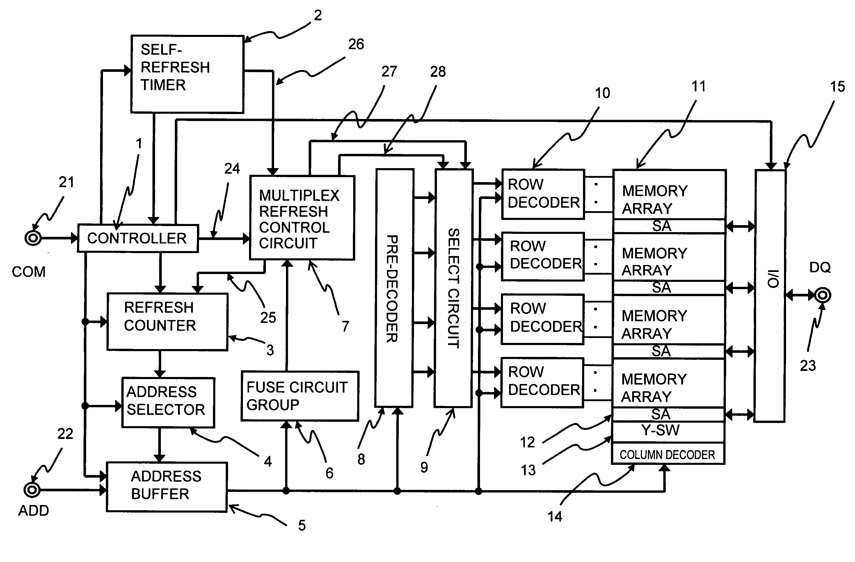
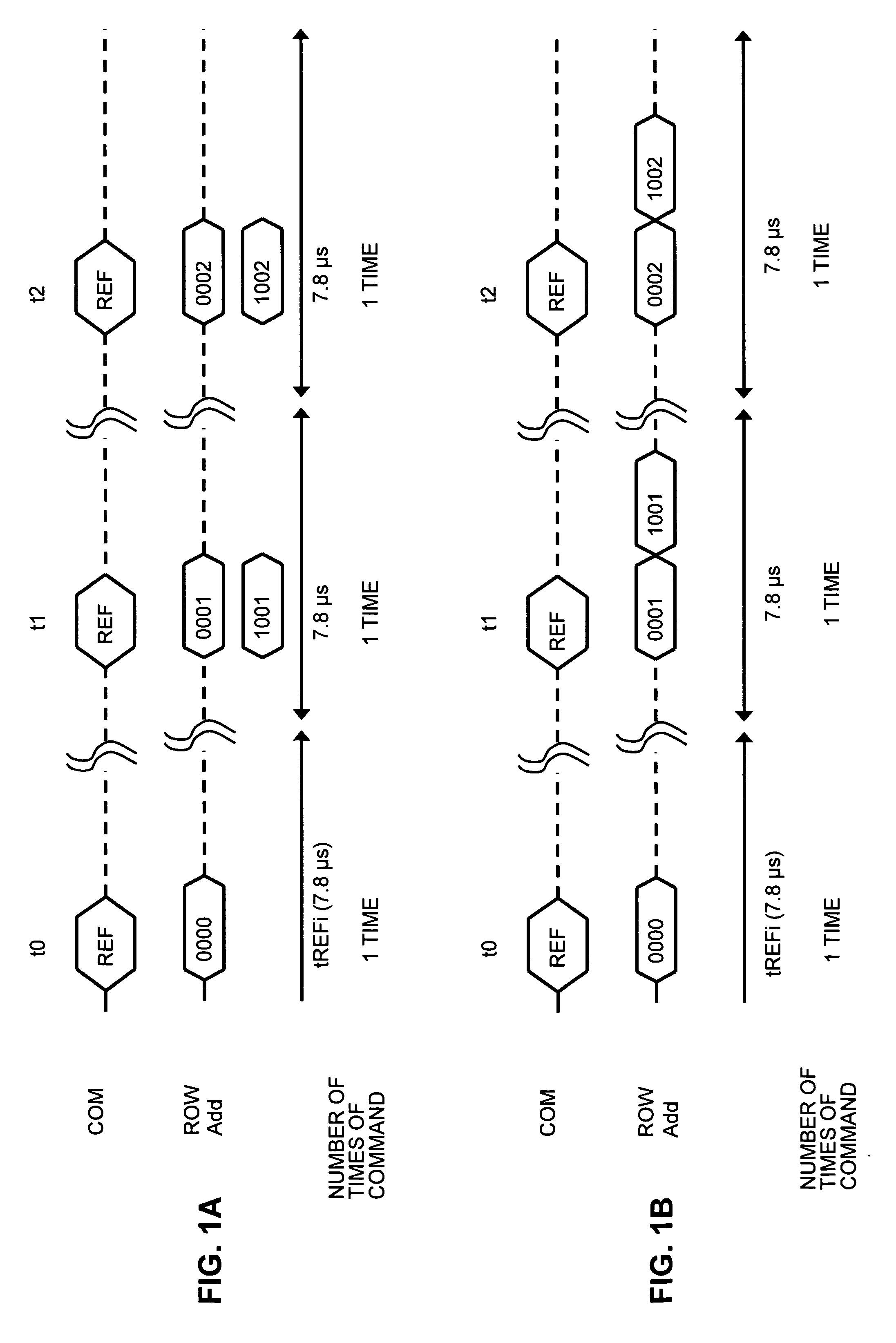
[0046] A first embodiment of the present invention will now be described with reference to FIGS. 1A, 1B and 5. In the present embodiment, double refresh is performed in distributed refresh, to save memory cells having short retention time. Distributed refresh is a manner of refresh in which a refresh command REF is input once at a maximum interval (tREFi). For example, the refresh commands are issued from a memory controller (outside the chip) every 7.8 μs. By comparison, a manner of refresh in which at least two refresh commands REF are input in succession at minimum intervals (tRFC) to perform continuous refresh is referred to as burst refresh. In burst refresh, the refresh commands are issued from a memory controller (outside the chip) every 105 ns, for example.

[0047] A multiplex refresh control circuit counts the number of refresh commands REF to identify distributed refresh or burst refresh as the manner of refresh. At this time, a self-refresh timer, which will be described l...

second embodiment

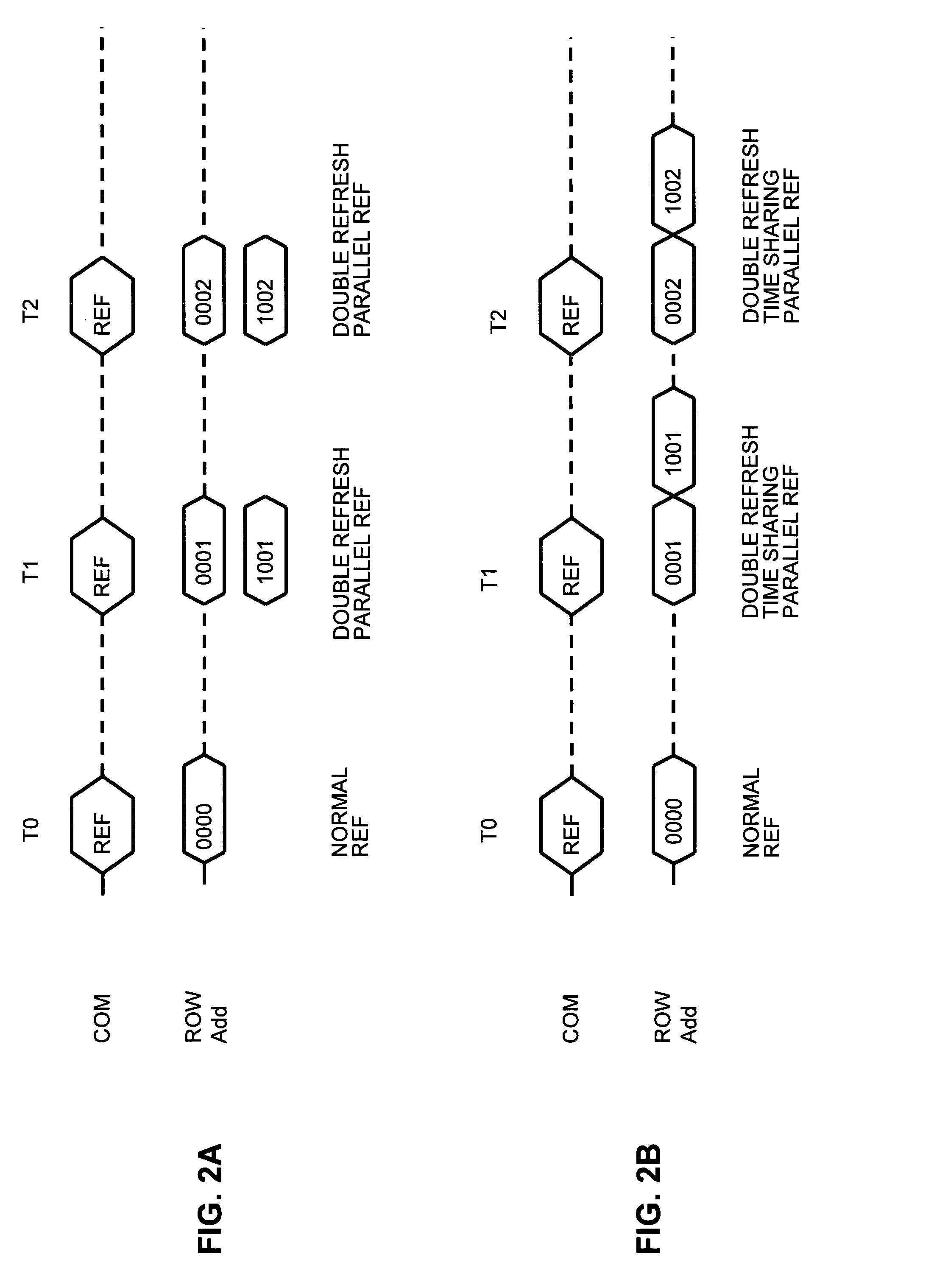
[0069] A second embodiment of the present invention will now be described with reference to FIGS. 2A, 2B and 5. In the present embodiment, double refresh is performed in burst refresh, to save memory cells having short retention time. FIG. 2A shows a timing chart of parallel refresh and FIG. 2 B shows a timing chart of time-sharing parallel refresh for double refresh performed within the same refresh cycle, according to the refresh method of the present embodiment. FIG. 5 is a schematic block diagram of the semiconductor device according to the present application. In FIG. 2, for the burst refresh, a plurality of refresh commands REF are consecutively input at minimum intervals (tRFC) within a maximum interval (tREFi) of 7.8 μs, to perform refresh operations. For the short period refresh, double refresh of the ½ period is carried out. The minimum interval (tRFC) may be 105 ns, for example, and up to eight refresh commands REF can be input in DDR2.

[0070] In FIG. 2A, refresh commands...

third embodiment

[0083] A third embodiment of the present invention will now be described with reference to FIGS. 3 and 5. In the present embodiment, in burst refresh, refresh commands (REF) are consecutively input at the minimum intervals (tRFC), and refresh is inserted into a next refresh cycle as double serial refresh. It is referred to as “double serial refresh” because the double refresh is inserted into the next refresh cycle. FIG. 3 shows a timing chart of the double serial refresh according to the present embodiment. FIG. 5 is a schematic block diagram of the semiconductor device according to the present application.

[0084] In the timing chart of FIG. 3, six refresh commands REF are input within the maximum interval (tREFi). At time T0, refresh command REF is input, and the word line of the first address “0000” is refreshed. At this time, the pair word line “1000” is not an object of double refresh, and thus, refresh is not carried out. At time T1, refresh command REF is input again, and the...


PUM


Abstract

Double refresh executing means is changed in accordance with a manner (distributed refresh or burst refresh) of a refresh command so as to suppress a drop of internal power supply that occurs upon double refresh.

Description

[0001] This application claims priority to prior Japanese patent application JP 2005-144942, the disclosure of which is incorporated herein by reference. BACKGROUND OF THE INVENTION [0002] 1. Field of the Invention [0003] The present invention relates to a semiconductor device, and more particularly to a semiconductor device capable of changing refresh cycles. [0004] 2. Description of the Related Art [0005] A dynamic random access memory (hereinafter, referred to as “DRAM”) is a kind of a semiconductor device that has large capacity and allows random accesses. DRAM stores information in the form of the charge amount stored in its capacitor, and thus, it requires a refresh operation to read and amplify the charge amount before it is lost so as to maintain the original state. The time (referred to as “information holding time” or “retention time”) until the charge amount stored in the capacitor of the memory cell in the DRAM is lost varies depending on memory cells. [0006] The memory ...

Claims


Application Information

Patent Timeline
IPC IPC(8): G11C7/00
CPCG11C11/40611G11C11/406
Inventor DONO, CHIAKIKOSHIKAWA, YASUJI
Owner LONGITUDE SEMICON S A R L
Why Eureka
Try Eureka