Semiconductor device

a semiconductor device and semiconductor technology, applied in the direction of transistors, basic electric elements, electrochemical generators, etc., can solve the problems of bringing about the increase of manufacturing costs or the large size of batteries, and achieve the effect of enhancing the performance of the semiconductor device and reducing the on resistance of the semiconductor devi

Inactive Publication Date: 2006-11-23
RENESAS ELECTRONICS CORP
View PDF6 Cites 44 Cited by
  • Summary
  • Abstract
  • Description
  • Claims
  • Application Information

AI Technical Summary

Benefits of technology

[0011] However, in the Li+ battery protective circuit shown in FIG. 36, when the above-mentioned pin arrangement is used, a portion of the wiring pattern 324 to which the source terminal S2 on the mounting substrate 323 is connected is narrowed and hence, the substrate wiring resistant is increased. Along with the increase of the substrate wiring resistance, a wiring loss is increased thus giving rise to a possibility that drawbacks such as the shortening of life time of the Li+ battery pack attributed to the generation of heat may be generated. Further, after pulling out the wiring pattern 324 to which the source terminal S2 is connected, it is necessary to increase a width of the wiring pattern 324 for reducing the substrate wiring resistance thus giving rise to a drawback that an area of the mounting substrate 323 is increased.
[0027] Further, the present invention also can enhance the performance of the semiconductor device.

Problems solved by technology

Accordingly, when the ON resistance is large, it is necessary to apply a design which enhances the heat radiation thus bringing about the increase of a manufacturing cost or the large-sizing of the battery as a whole or a battery protective circuit.

Method used


Image

  • Semiconductor device
  • Semiconductor device
  • Semiconductor device

Examples


embodiment 1

[0068] The semiconductor device according to the embodiments of the present invention will be explained with reference to the drawings.

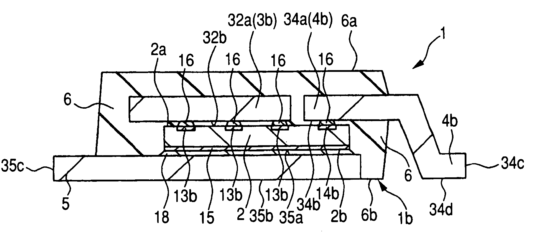
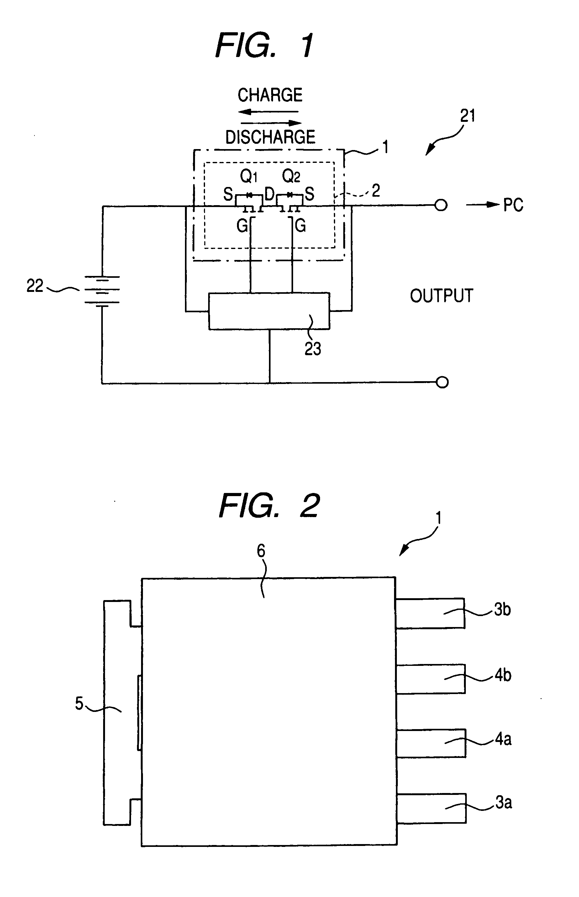
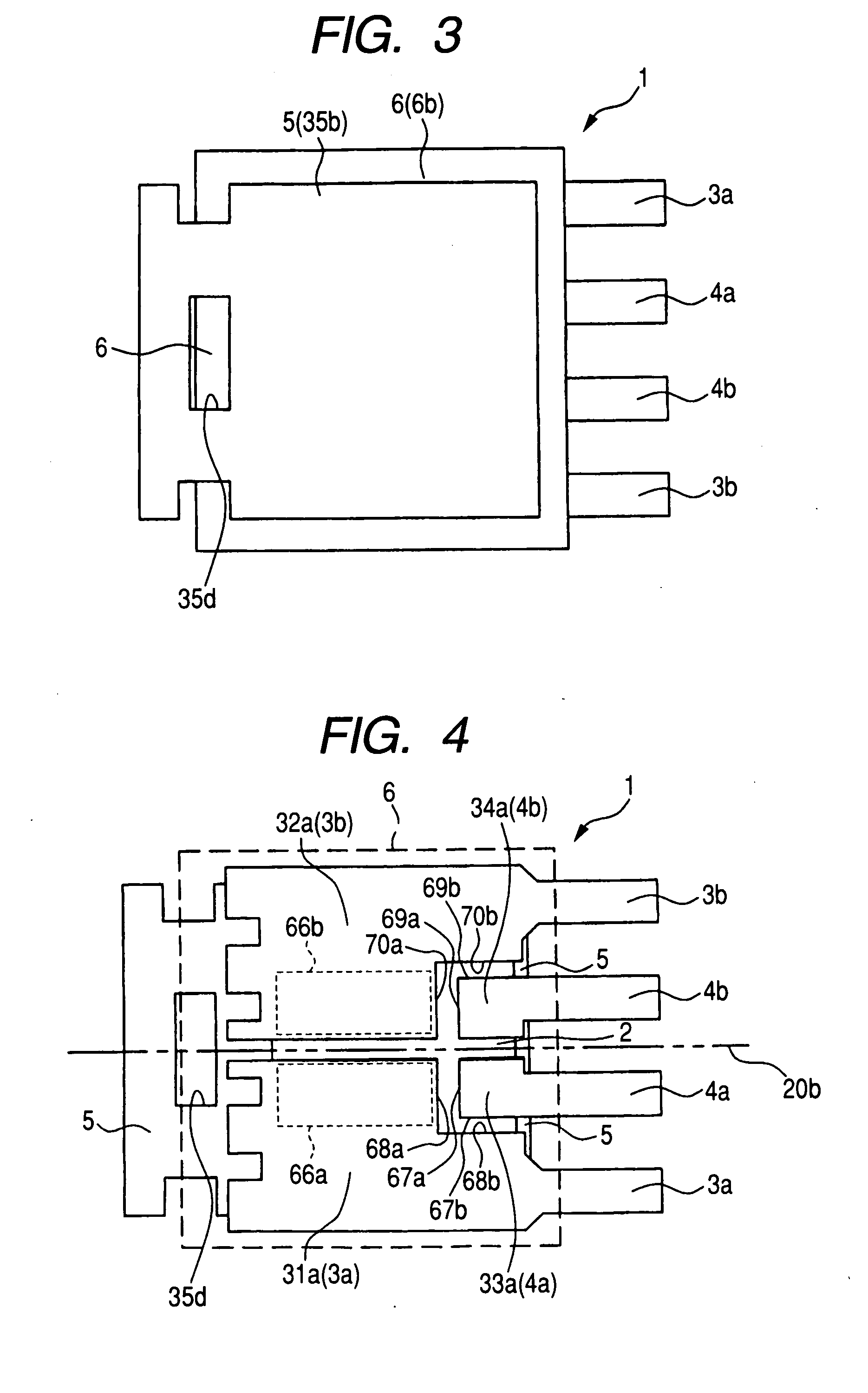
[0069]FIG. 1 is a circuit diagram of a Li+ battery pack using a semiconductor device 1 according to an embodiment of the present invention. FIG. 2 is a top plan view (a plan view) of the semiconductor device 1 according to the embodiment of the present invention, FIG. 3 is a bottom plan view (a back view) of the semiconductor device 1, FIG. 4 and FIG. 5 are perspective plan views of the semiconductor device 1, and FIG. 6 to FIG. 9 are cross-sectional views (cross-sectional side views) of the semiconductor device 1. Here, FIG. 4 corresponds to the top plan view of the semiconductor device 1 when a resin sealing portion 6 is observed in a see-through manner, and FIG. 5 corresponds to the top plan view of the semiconductor device 1 when the resin sealing portion 6, source terminals 3a and 3b, and gate terminals 4a and 4b are observed in a see-through m...

embodiment 2

[0151] In the above-mentioned embodiment 1, the source electrodes 13a, 13b and the gate electrodes 14a, 14b of the semiconductor chip 2 are electrically connected with the source terminals 3a, 3b and the gate terminals 4a, 4b via the bump electrode 16. In this embodiment, source electrodes 13a, 13b and gate electrodes 14a, 14b of a semiconductor chip 2c are electrically connected with source terminals 3a, 3b and gate terminals 4a, 4b via a conductive bonding material 71.

[0152]FIG. 25 is a perspective plan view of the semiconductor device 1c according to this embodiment and FIG. 26 and FIG. 27 are cross-sectional views (cross-sectional side views) of the semiconductor device 1c. Here, FIG. 25 corresponds to a top plan view of the semiconductor device 1c in a state that a resin sealing portion 6, source terminals 3a, 3b and gate terminals 4a, 4b are observed in a see-through manner and corresponds to FIG. 5 of the above-mentioned embodiment 1. Further, a cross section of the semicond...

embodiment 3

[0161] In the above-mentioned embodiment 1, portions of source terminals 3a, 3b, and gate terminals 4a, 4b are projected from a side face of a resin sealing portion 6, and these terminals function as an external terminal. That is, the semiconductor device 1 of the above-mentioned embodiment 1 is a lead-type semiconductor package. The source terminals 3a, 3b, and the gate terminals 4a, 4b are not projected from the resin sealing portion 6 and hence, a semiconductor device 1d of this embodiment is a non-lead type (leadless type) semiconductor package.

[0162]FIG. 28 is a bottom plan view (back view) of the semiconductor device 1d of this embodiment, and FIG. 29 and FIG. 30 are cross-sectional views (cross-sectional side views) of the semiconductor device 1d. FIG. 28 to FIG. 30 correspond to FIG. 3, FIG. 6, and FIG. 7 of the above-mentioned embodiment 1, respectively. In addition, a cross section of the semiconductor device 1d at a position taken along a line H-H in FIG. 28 corresponds ...


PUM


Abstract

Two vertical-type power MISFETs are formed over a semiconductor chip, a common drain electrode formed over a back surface of the semiconductor chip is electrically connected with a drain terminal via a conductive bonding material, source electrodes and gate electrodes formed over a surface of the semiconductor chip are respectively electrically connected with source terminals and gate terminals via bump electrodes, and these components are sealed by a resin sealing portion. The exposed portions of the gate terminals are arranged inside the resin sealing portion, and the exposed portions of the source terminals are arranged outside the resin sealing portion. The source terminals extend over the surface of the semiconductor chip and are connected with the source electrodes which are uniformly arranged over regions of the surface of the semiconductor chip except for gate electrode forming regions and the vicinities of these regions via the bump electrodes.

Description

CROSS-REFERENCE TO RELATED APPLICATION [0001] The present application claims priority from Japanese patent application No. 2005-144076 filed on May 17, 2005, the content of which is hereby incorporated by reference into this application. BACKGROUND OF THE INVENTION [0002] The present invention relates to a semiconductor device, and more particularly to a technique which is effectively applicable to a semiconductor device having field effect transistors which are used as charge / discharge switching elements of a battery or the like. [0003] In a portable equipment as represented by a notebook-type PC or a mobile phone, a Li ion (hereinafter referred to as Li+) battery which possesses high energy density is generally used as a battery which supplies an electric power. A power MISFET is connected with the Li+ battery as a switching element, and the power MISFET controls the Li+ battery by controlling charging and discharging of the battery. [0004] In Japanese Patent Laid-open 2004-356499...

Claims


Application Information

Patent Timeline
Patent Type & Authority Applications(United States)
IPC IPC(8): H01L21/336H01L29/76
CPCH01L23/3107H01L23/49562H01L2924/1306H01L2224/73253H01L2224/32245H01L2224/16245H01L2924/01033H01L2924/01023H01L2924/01019H01L2924/01006H01L24/48H01M10/46H01M10/052H01L2924/14H01L24/06H01L24/36H01L24/40H01L24/49H01L27/088H01L29/66727H01L29/66734H01L29/7811H01L29/7813H01L2224/0401H01L2224/04042H01L2224/0603H01L2224/13144H01L2224/48247H01L2224/48472H01L2224/49111H01L2924/01003H01L2924/01004H01L2924/01005H01L2924/01013H01L2924/01014H01L2924/01015H01L2924/01022H01L2924/01028H01L2924/01029H01L2924/01047H01L2924/01074H01L2924/01078H01L2924/01079H01L2924/01082H01L2924/014H01L2924/13091H01L2924/00H01L2924/181H01L2924/00014H01L2224/37147H01L2224/83801H01L24/37H01L2224/37599H01L2224/84801H01L2224/371H01L2224/8385Y02E60/10H01L2224/45099H01L2924/00012H01L2224/05599H01L2224/73221
Inventor TAKAHASHI, HIROYUKIKOYANO, MASASHI
Owner RENESAS ELECTRONICS CORP
Why Eureka
Try Eureka