On-chip apparatus and method for determining integrated circuit stress conditions

a technology of stress conditions and integrated circuits, applied in the field of semiconductor integrated circuits, can solve problems such as reducing the life of integrated circuits, increasing the reliability margin of integrated circuits, and affecting the reliability of integrated circuits

Inactive Publication Date: 2006-11-30
AGERE SYST INC
View PDF19 Cites 44 Cited by
  • Summary
  • Abstract
  • Description
  • Claims
  • Application Information

AI Technical Summary

Problems solved by technology

Power supply voltage and / or temperature excursions outside design limits can cause immediate failure or reduce integrated circuit life.
It is generally known that design or process modifications can be implemented to extend the supply voltage and temperature tolerance, thereby increasing the reliability margin of the integrated circuit, but at the expense of increased fabrication costs.
Changes in manufacturing processes and the continual progression to smaller and denser devices may contribute to an erosion of the reliability margin, resulting in increased risk of premature chip failure.
As semiconductor integrated circuits are scaled to smaller dimensions, the requirement to maintain operation within the power supply voltage and temperature limits becomes more critical.
Failure of an integrated circuit embedded within a system will likely cause a failure of the system, an unfortunate outcome that can be expensive and disruptive to the system user.
For example, failure of a disk drive requires purchase of a replacement drive and entails a data recovery cost.
Consequential losses such as data recovery can be costly and can easily exceed the hardware replacement cost.
However, redundant systems incur an extra cost, i.e., a doubled cost.
Generally, when an integrated circuit fails in the field and is returned to the supplier for a failure analysis, it is difficult for the chip supplier to determine the failure's root cause, especially since the supplier lacks knowledge of voltage or temperature stresses or other operational abuses to which the integrated circuit may have been exposed during operation.

Method used


Image

  • On-chip apparatus and method for determining integrated circuit stress conditions
  • On-chip apparatus and method for determining integrated circuit stress conditions
  • On-chip apparatus and method for determining integrated circuit stress conditions

Examples


Embodiment Construction

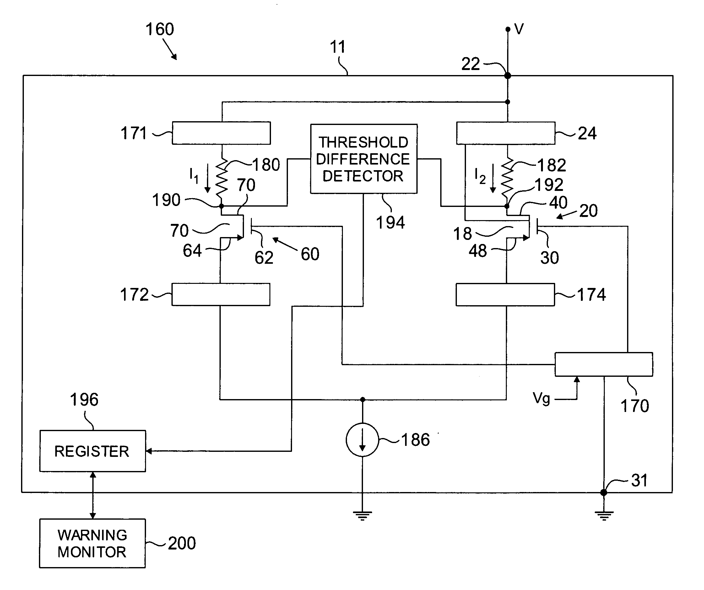
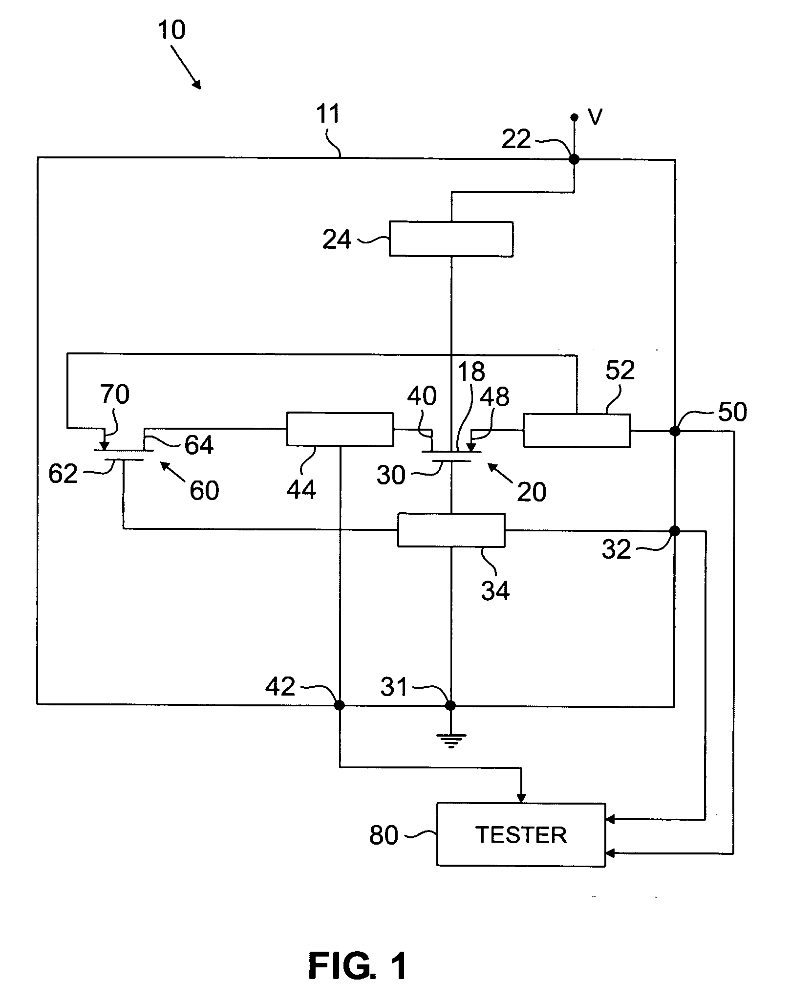
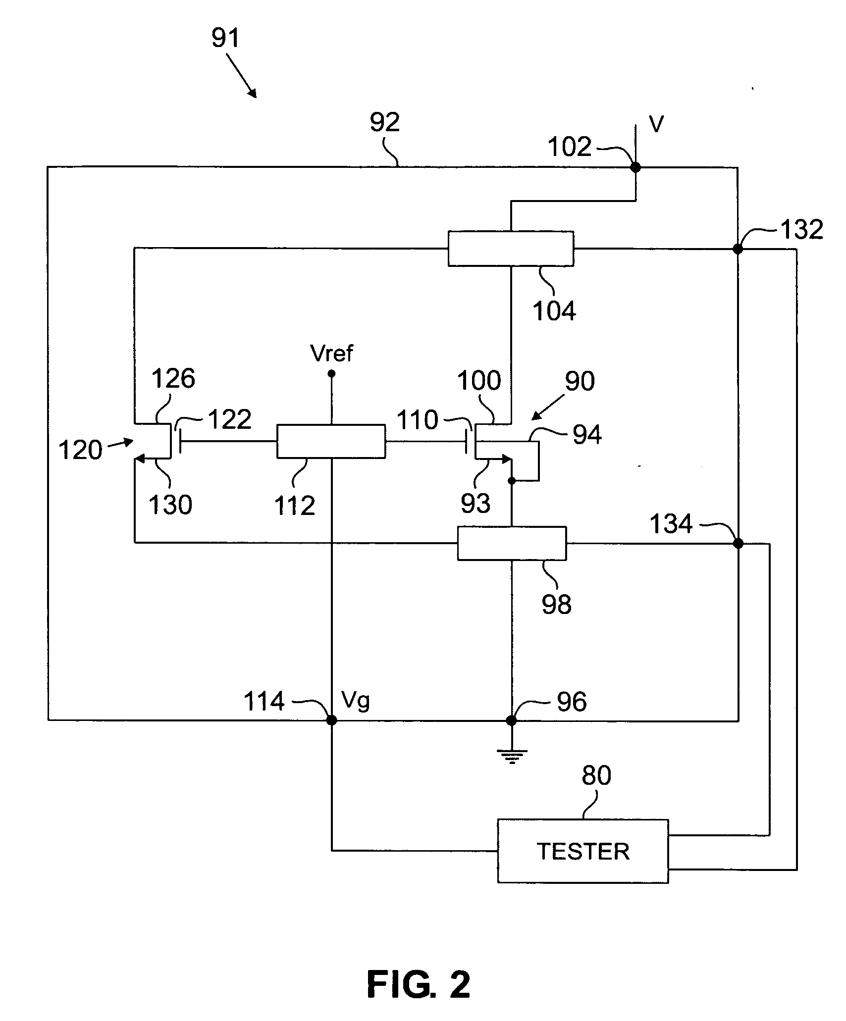
[0015] Before describing in detail the particular on-chip power supply and temperature monitoring process and apparatus according to the present invention, it should be observed that the present invention resides in a novel and non-obvious combination of hardware elements and process steps. Accordingly, these elements have been represented by conventional elements in the drawings and specification, wherein elements and process steps conventionally known in the art are described in lesser detail, and elements and steps pertinent to understanding the invention are described with greater detail.

[0016] As is known, exposure of an integrated circuit or components thereof, to an excessive power supply voltage and / or an excessive operating temperature may cause device failure or reduce the device's operating life due to premature aging. One specific observable effect of these stressed operating conditions is a threshold voltage shift in the MOSFETS of the integrated circuit.

[0017] An exc...


PUM


Abstract

A method and apparatus for determining whether an integrated circuit has been subjected to stress conditions during operation. The integrated circuit comprises a test device that is exposed to the same power supply voltage and temperature as other devices in the integrated circuit. Certain expected operating parameters, as a function of the operating life of the integrated circuit, are predetermined. If a measured value of the operating parameter exceeds the expected value then the integrated circuit has been subjected to stress conditions.

Description

FIELD OF THE INVENTION [0001] This invention relates generally to semiconductor integrated circuits, and more particularly to an apparatus and method for monitoring one or both of an integrated circuit temperature and a power supply voltage supplied to the integrated circuit. BACKGROUND OF THE INVENTION [0002] Integrated circuits (or chips) typically comprise a silicon substrate with semiconductor devices, such as transistors, formed from doped regions within the substrate. Interconnect structures, also referred to as metallization layers, comprising substantially parallel conductive layers connected by substantially vertical conductive vias, provide electrical connection between doped regions to form electrical circuits within the integrated circuit. Typically several metallization layers are required to interconnect the doped regions in the integrated circuit. The top metallization layer provides attachment sites for receiving conductive interconnects (e.g., bond wires) that conne...

Claims


Application Information

Patent Timeline
Patent Type & Authority Applications(United States)
IPC IPC(8): G01R31/26
CPCG01R31/2884
Inventor HARRIS, EDWARD B.AYUKAWA, MICHAEL C.MASON, PHILIP W.HUI, FRANK YAUCHEE
Owner AGERE SYST INC
Why Eureka
Try Eureka