Isolation process and structure for CMOS imagers

Active Publication Date: 2006-11-30
APTINA IMAGING CORP
View PDF8 Cites 28 Cited by
  • Summary
  • Abstract
  • Description
  • Claims
  • Application Information

AI Technical Summary

Benefits of technology

[0012] In one aspect, the invention provides a barrier implanted region of a first conductivity type formed in lieu of an isolation region of a pixel sensor cell that provides physical and electrical isolation of photosensors of adjacent pixel sensor cells of a CMOS imager. The barrier implanted region comprises a first region having a first width and a second region located below the first region and having a second width greater than the

Problems solved by technology

Another problem associated with the formation of the above-described trench isolation regions 15 is that, when ions are implanted in the substrate close to bottom 17 and edges or sidewalls 16 (FIG. 2) of the trench, current leakage can occur at the junction between the active device regions and the trench.
Current generated from trap sites inside or near the photodiode depletion region als

Method used


Image

  • Isolation process and structure for CMOS imagers
  • Isolation process and structure for CMOS imagers
  • Isolation process and structure for CMOS imagers

Examples


Example

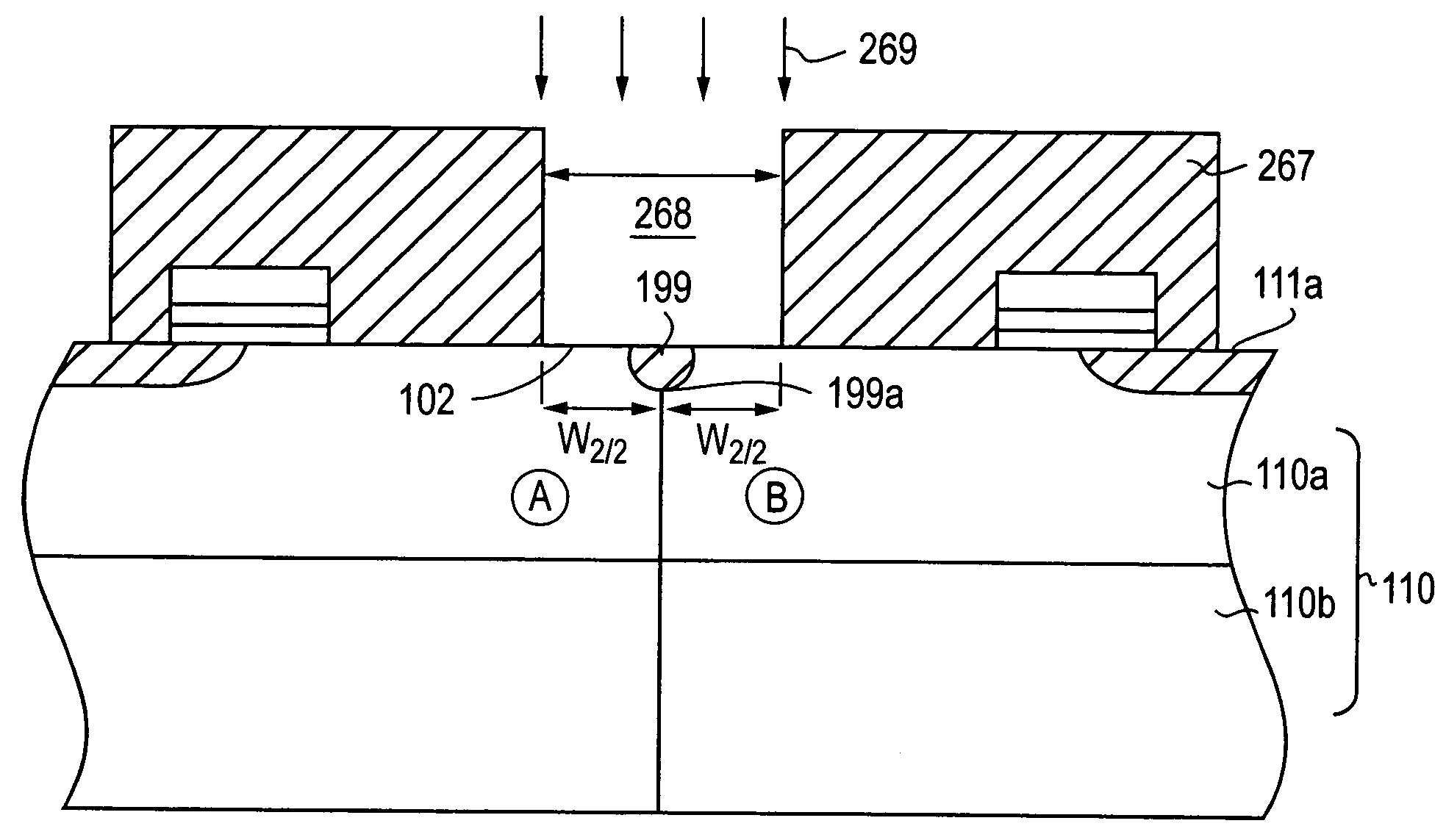
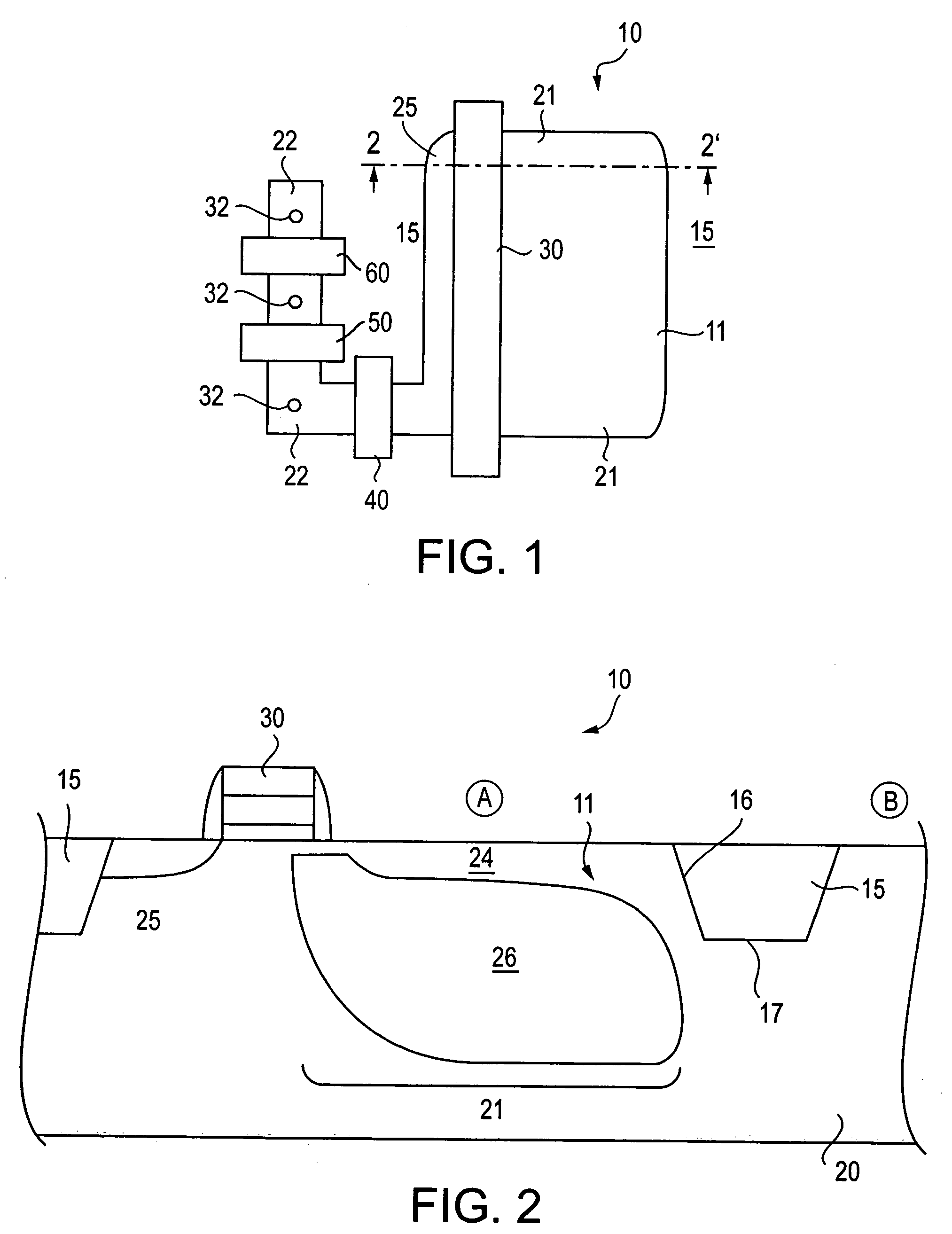
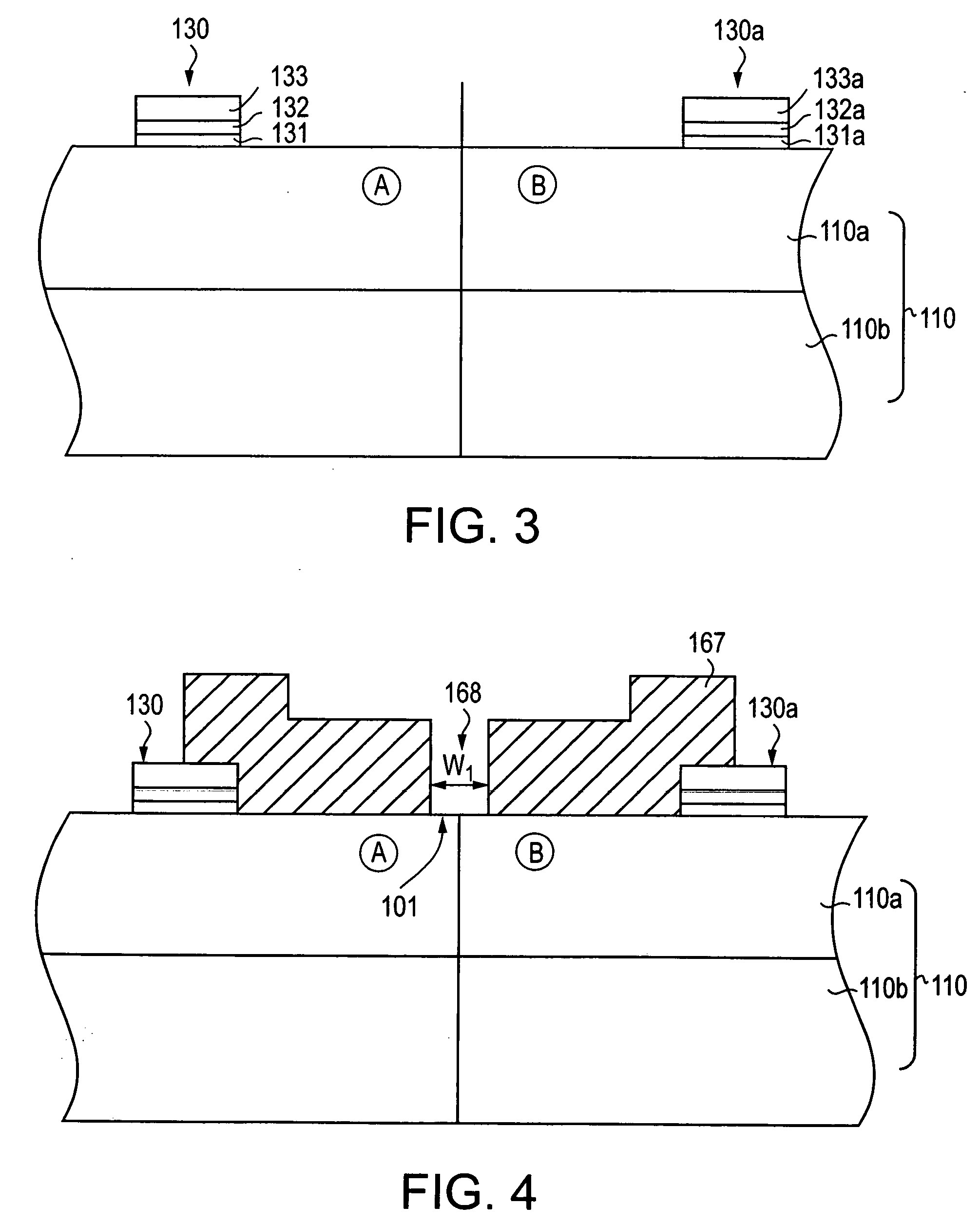
[0026] In the following detailed description, reference is made to the accompanying drawings which form a part hereof, and in which is shown by way of illustration specific embodiments in which the invention may be practiced. These embodiments are described in sufficient detail to enable those skilled in the art to practice the invention, and it is to be understood that other embodiments may be utilized, and that structural, logical and electrical changes may be made without departing from the spirit and scope of the present invention.

[0027] The terms “wafer” and “substrate” are to be understood as a semiconductor-based material including silicon, silicon-on-insulator (SOI) or silicon-on-sapphire (SOS) technology, doped and undoped semiconductors, epitaxial layers of silicon supported by a base semiconductor foundation, and other semiconductor structures. Furthermore, when reference is made to a “wafer” or “substrate” in the following description, previous process steps may have be...


PUM


Abstract

A barrier implanted region of a first conductivity type formed in lieu of an isolation region of a pixel sensor cell that provides physical and electrical isolation of photosensitive elements of adjacent pixel sensor cells of a CMOS imager. The barrier implanted region comprises a first region having a first width and a second region having a second width greater than the first width, the second region being located below the first region. The first region is laterally spaced from doped regions of a second conductivity type of adjacent photodiodes of pixel sensor cells of a CMOS imager.

Description

FIELD OF THE INVENTION [0001] The present invention relates to the field of semiconductor devices and, in particular, to high quantum efficiency CMOS image sensors. BACKGROUND OF THE INVENTION [0002] CMOS imagers are known in the art. A top-down view of a semiconductor wafer fragment of an exemplary CMOS sensor pixel four-transistor (4T) cell 10 is illustrated in FIG. 1. As it will be described below, the CMOS sensor pixel cell 10 includes a photo-generated charge accumulating area 21 in an underlying portion of the substrate. This area 21 is formed as a pinned diode 11 (FIG. 2). The pinned photodiode is termed “pinned” because the potential in the photodiode is pinned to a constant value when the photodiode is fully depleted. It should be understood, however, that the CMOS sensor pixel cell 10 may include a photogate or other image to charge converting device, in lieu of a pinned photodiode, as the initial accumulating area 21 for photo-generated charge. [0003] The CMOS image senso...

Claims


Application Information

Patent Timeline
IPC IPC(8): H01L21/00
CPCH01L27/14603H01L27/1463H01L27/14689H01L27/14683H01L27/14643H01L27/146
Inventor BRADY, FREDERICKPATRICK, INNA
Owner APTINA IMAGING CORP
Why Eureka
Try Eureka