High speed electron tunneling devices

a technology of electron tunneling and high-speed, applied in the field of optical devices, can solve the problems of impracticality of semiconductor-based devices, limited efficiency of such devices, and small size of electronic devices

Inactive Publication Date: 2006-12-07
UNIV OF COLORADO THE REGENTS OF
View PDF82 Cites 40 Cited by
  • Summary
  • Abstract
  • Description
  • Claims
  • Application Information

AI Technical Summary

Problems solved by technology

However, prior art M-I-M devices generally exhibit low degrees of asymmetry and nonlinearity in the electron transport such that the efficiency of such devices is limited.
It has been suggested that the recent trend of decreasing the size of electronic devices to achieve high speed switching will ultimately make semiconductor-based devices impractical due to fluctuation of carrier concentration, which occurs when semiconductor devices are reduced to mesoscopic regimes (see, for example, Suemasu, et al., “Metal (CoSi2) / Insulator(CaF2) resonant tunneling diode,”Japanese Journal of Applied Physics, vol.
In other words, the response of the semiconductor device is limited by the bandgap energy.
When a semiconductor diode is used to rectify high frequency oscillations, the semiconductor material limits the frequency response of the diode because the charge carriers must be transported through a band, in which concentration are limited in comparison to a metal.
However, the M-I-M-I-M-I-M device of Suemasu is much more complicated than the simple M-I-M devices, and must be fabricated using a complex epitaxial growth procedure using exotic materials.
Therefore, although the M-I-M-I-M-I-M device of Suemasu achieves much higher degrees of asymmetry and nonlinearity in the I-V curve than the M-I-M devices, the performance gains come at the cost of the simplicity in design and fabrication.
The drawback to currently available MIS devices is also the limited efficiency due to asymmetry and nonlinearity limitations.
MIS devices cannot operate at as high frequencies as M-I-M devices because the concentration of electron states in the semiconductor is lower than that from a metal.
At this time, infrared detectors, for example, capable of receiving electromagnetic signal at terahertz rates, at room temperature, are not readily available, to the Applicants' knowledge.
Temperature-controlled alternatives, such as narrow bandgap semiconductor detectors, and bolometers, exist on the market, but the extra considerations associated with the temperature control mechanism make such devices expensive and bulky.
Prior art M-I-M detectors are capable of detecting infrared radiation without cooling, but these prior art detectors are not sensitive enough for practical applications.
This arrangement includes a first layer of an amorphous material such that using only the first layer of amorphous material in the arrangement would result in a given degree of nonlinearity in the transport of electrons, with respect to the given voltage.

Method used


Image

  • High speed electron tunneling devices
  • High speed electron tunneling devices
  • High speed electron tunneling devices

Examples


Embodiment Construction

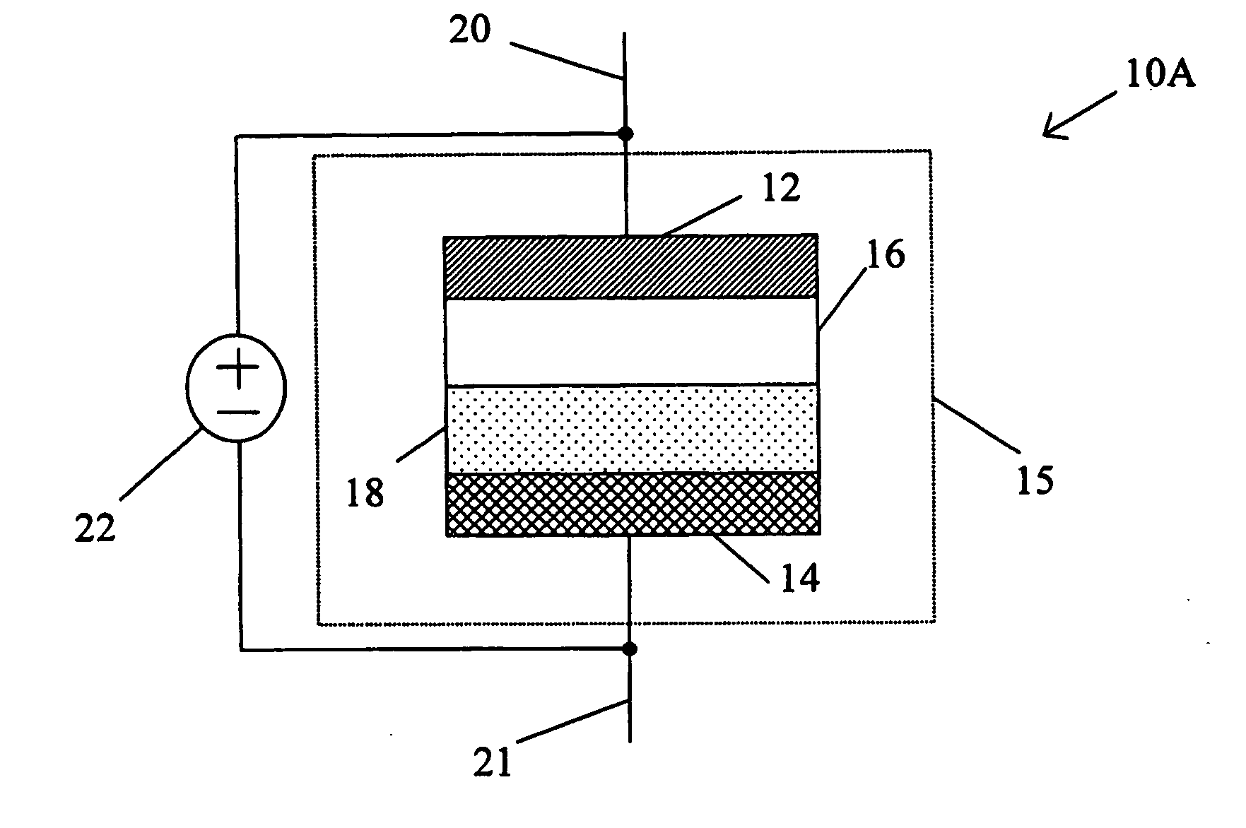
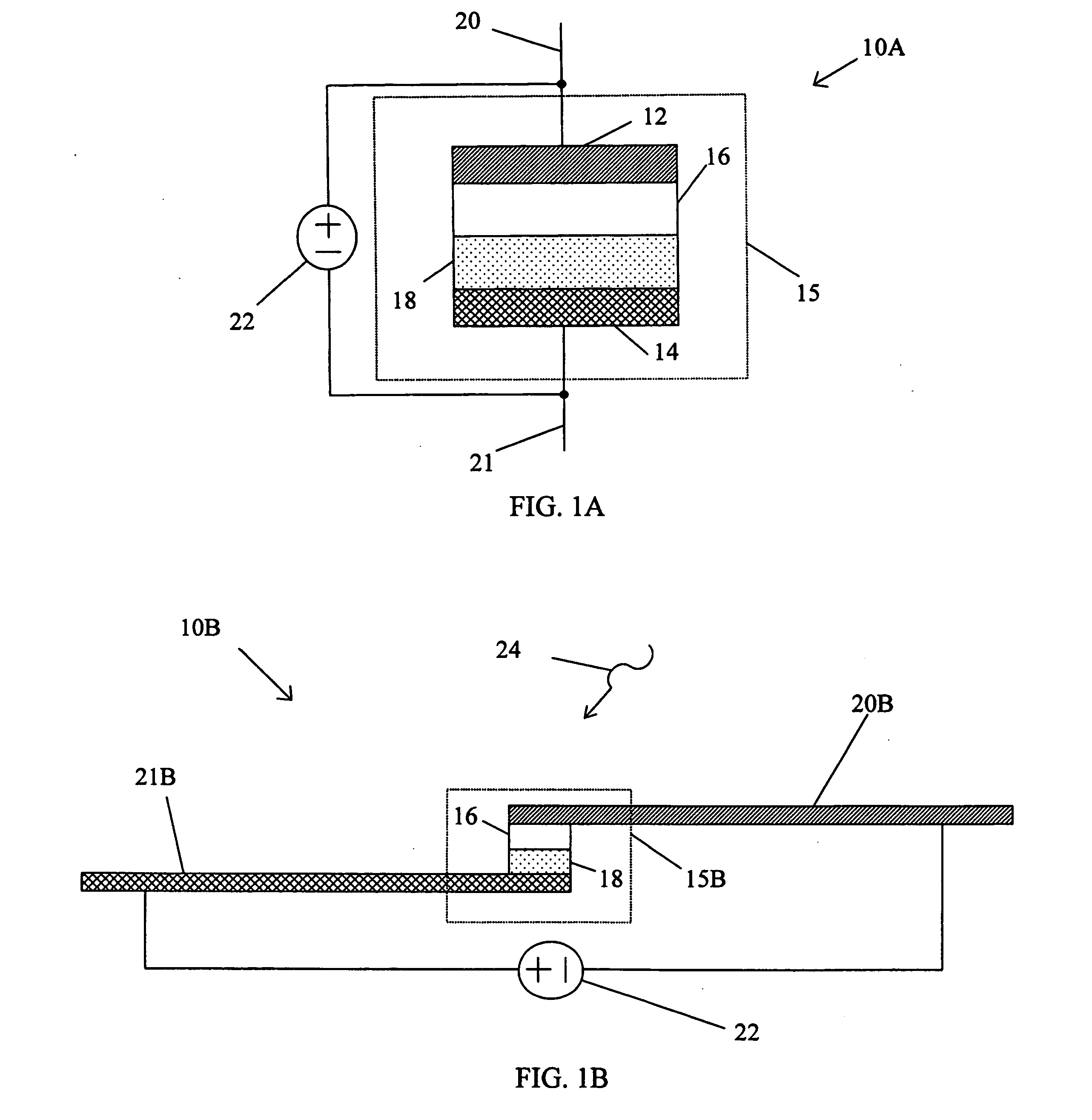
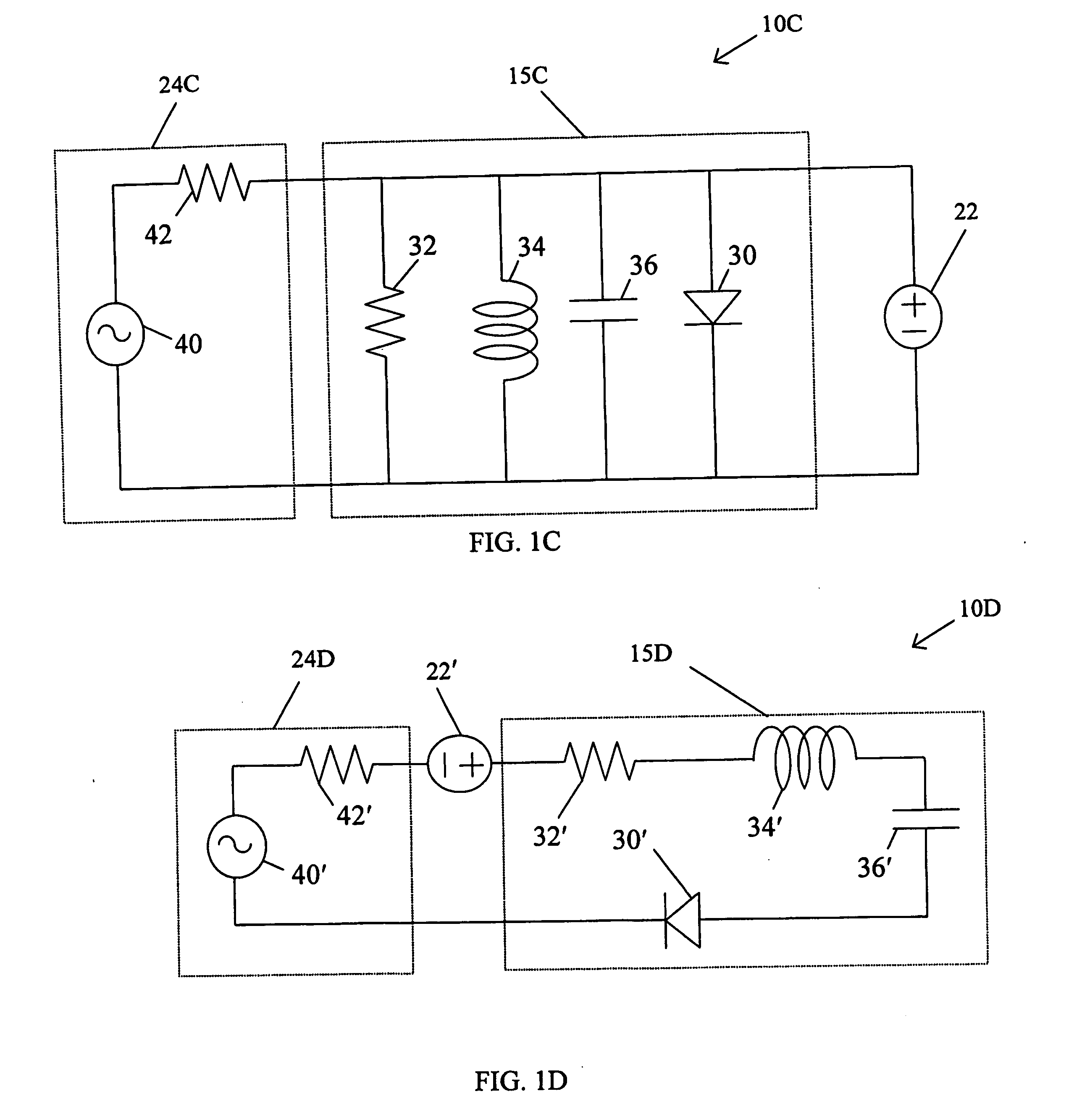
[0037] Still another alternative to the M-I-M, M-I-M-I-M-I-M and MIS devices is disclosed in copending U.S. patent application Ser. No. 09 / 860,988 Attorney Docket Number Phiar-P001 of Eliasson and Moddel (Eliasson), which is filed contemporaneously herewith and is incorporated herein by reference. Eliasson discloses an electron tunneling device based on metal-oxide combinations similar to an M-I-M structure but including additional layer of an insulator positioned between the non-insulating layers. The additional layer of Eliasson is configured to increase the nonlinearity, asymmetry and differential resistance exhibited by the resulting device over and above the values of these parameters exhibited by a simple M-I-M device, which does not include the additional layer. The concept of tailoring the layering of the non-insulating and insulating layers within the electron tunneling device can be extended to achieve heretofore unseen optoelectronic devices such as narrowband detectors, ...


PUM


Abstract

A detector includes a voltage source for providing a bias voltage and first and second non-insulating layers, which are spaced apart such that the bias voltage can be applied therebetween and form an antenna for receiving electromagnetic radiation and directing it to a specific location within the detector. The detector also includes an arrangement serving as a transport of electrons, including tunneling, between and to the first and second non-insulating layers when electromagnetic radiation is received at the antenna. The arrangement includes a first insulating layer and a second layer configured such that using only the first insulating in the arrangement would result in a given value of nonlinearity in the transport of electrons while the inclusion of the second layer increases the nonlinearity above the given value. A portion of the electromagnetic radiation incident on the antenna is converted to an electrical signal at an output.

Description

RELATED APPLICATION [0001] The present application is a Continuation of U.S. patent application Ser. No. 10 / 877,874, filed on Jun. 26, 2004; which is a Continuation of U.S. patent application Ser. No. 10 / 347,534, filed on Jan. 20, 2003 and issued as U.S. Pat. No. 6,756,649 on Jun. 29, 2004; which is a Continuation of U.S. patent application Ser. No. 09 / 860,972, filed on May 21, 2001 and issued as U.S. Pat. No. 6,563,185 on May 13, 2003; all of which are incorporated herein by reference in their entirety.BACKGROUND OF THE INVENTION [0002] The present invention relates generally to optical devices and, more particularly, to optoelectronic devices based on electron tunneling. [0003] The increasing speed of optical communications is fueling the race to achieve ever faster optical communications devices for transmitting, modulating and detecting electromagnetic signals. Terahertz speeds are expected in the near future, and optical communication devices that can operate at such high speed...

Claims


Application Information

Patent Timeline
Patent Type & Authority Applications(United States)
IPC IPC(8): H01L29/08H01L27/144H01L29/73H01L29/76H01L29/82H01L31/08H01L39/22H01L45/00
CPCB82Y10/00B82Y15/00B82Y20/00H01L27/1446H01L29/7311H01L29/7606H01L45/00H01L31/08H01L31/101H01L33/0004H01L33/0037H01L39/22H01L29/82H10N60/10H10N70/00
Inventor MODDEL, GARRETELIASSON, BLAKE J.
Owner UNIV OF COLORADO THE REGENTS OF
Why Eureka
Try Eureka