Transistor for memory device and method for manufacturing the same

Active Publication Date: 2006-12-07
SK HYNIX INC
View PDF4 Cites 41 Cited by
  • Summary
  • Abstract
  • Description
  • Claims
  • Application Information

AI Technical Summary

Benefits of technology

[0008] Accordingly, the present invention has been made to solve the above-mentioned problems occurring in the prior art, and an object of the present invention is to provide a transistor for a memory device reali

Problems solved by technology

However, three-dimensionally structured transistors have a problem in that they cannot secure enough data retention time, which is the most important property cells must have.
In summary, although conventional fin transisto

Method used


Image

  • Transistor for memory device and method for manufacturing the same
  • Transistor for memory device and method for manufacturing the same
  • Transistor for memory device and method for manufacturing the same

Examples


Example

[0022] Hereinafter, a preferred embodiment of the present invention will be described with reference to the accompanying drawings. In the following description and drawings, the same reference numerals are used to designate the same or similar components, and so repetition of the description on the same or similar components will be omitted.

[0023] A method for manufacturing a transistor for a memory device according to the present invention will now be described with reference to FIGS. 1 to 7, which show the respective processes thereof.

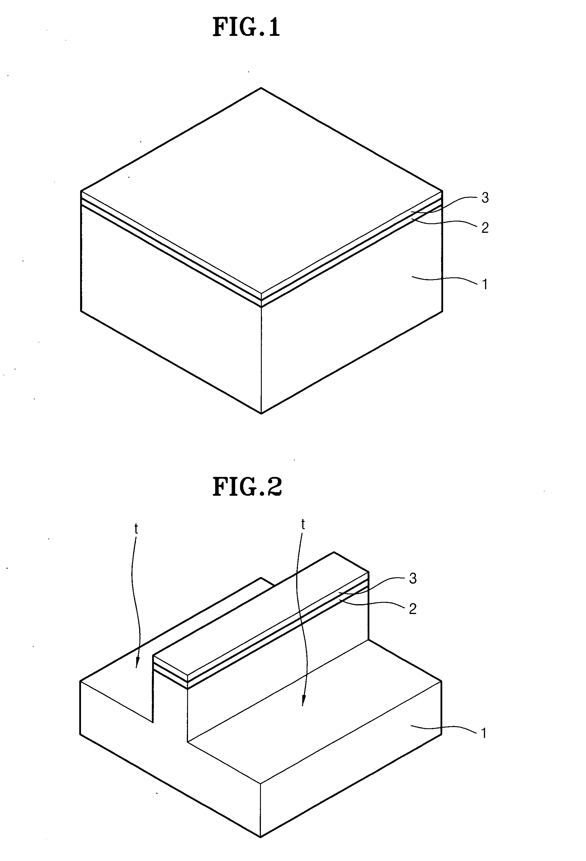
[0024] Referring to FIG. 1, a pad oxide layer 2 and a pad nitride layer 3 are successively formed on a semiconductor substrate 1 with a thickness of 50-150 Å and 500-800 Å, respectively.

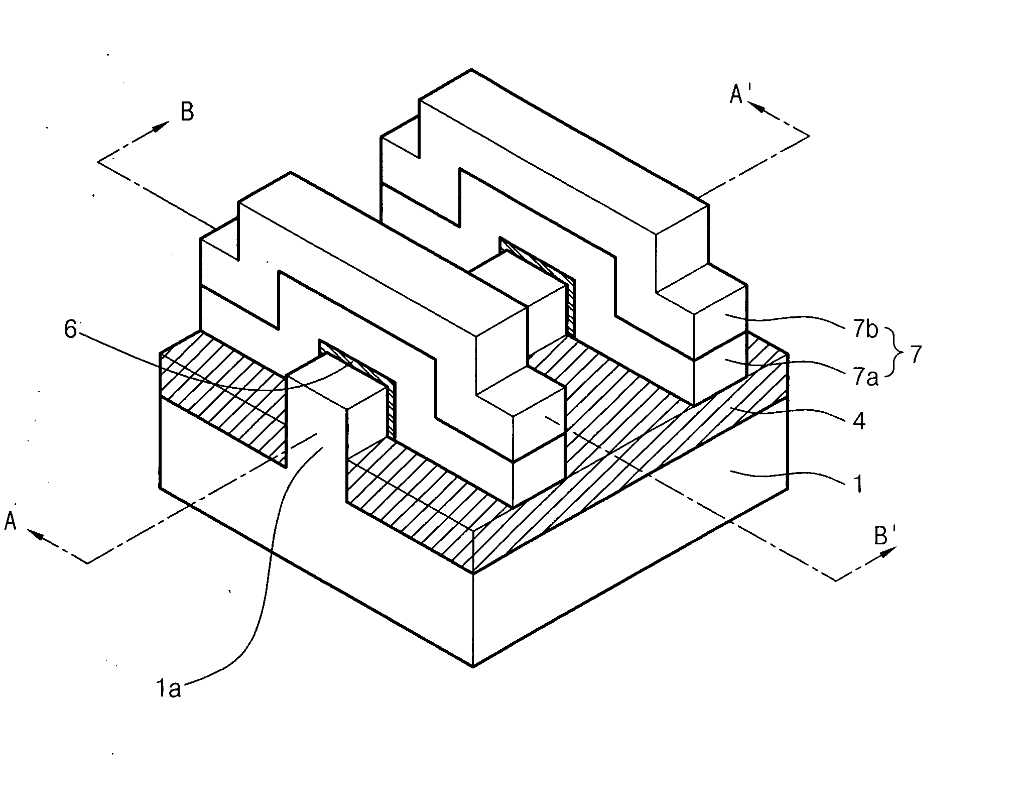
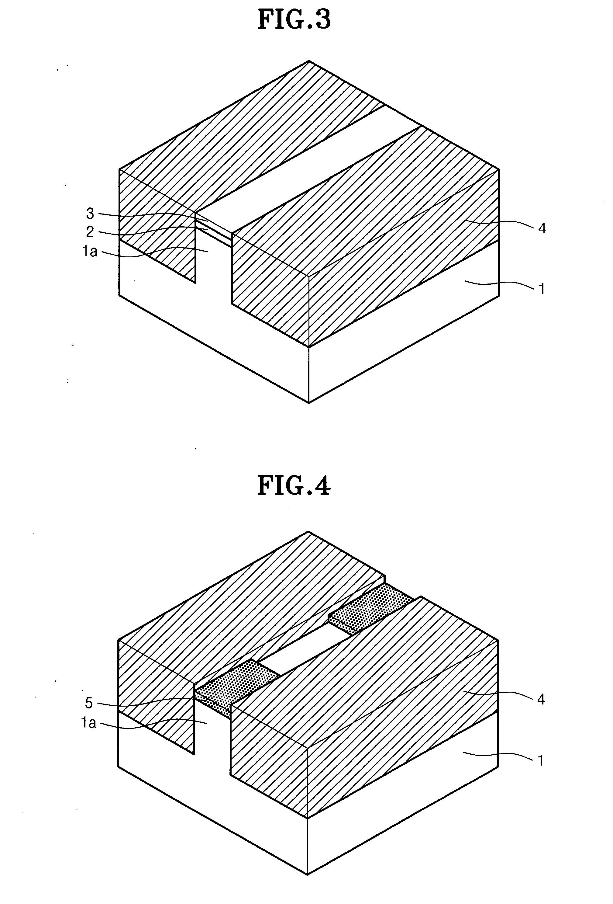
[0025] Referring to FIG. 2, trenches t are formed by etching the pad nitride layer 3, the pad oxide layer 2, and the substrate 1 to a predetermined depth with a mask delimiting portions on which trenches are to be formed. As a result, an active region 1a protruding...


PUM


Abstract

Disclosed is a transistor for a memory device realizing both a step-gated asymmetry transistor and a fin transistor in a cell and a method for manufacturing the same. The transistor has an active region protruding from a predetermined region of a substrate and a groove formed in the active region. A field oxide layer is formed on the substrate around the active region in such a manner that it has a surface lower than the upper surface of the active region including the groove. A pair of gates are placed along one and the other ends of groove across the upper surface of the active region while overlapping the stepped portion of the active region. The transistor has the structure of a step-gated asymmetry transistor when seen in a sectional view taken in a first direction, as well as that of a fin transistor when seen in a sectional view taken in a second direction, which is perpendicular to the first direction. The transistor having such a structure can secure improved data retention time of the step-gated asymmetry transistor and excellent current driving properties of the fin transistor and is applicable not only to a logic device, but also to a memory device (for example, DRAM) requiring low-power and high-speed properties.

Description

BACKGROUND OF THE INVENTION [0001] 1. Field of the invention [0002] The present invention relates to a memory device and a method for manufacturing the same, and more particularly to a new type of transistor realizing both a fin transistor and a step-gated asymmetry transistor in a unit cell and a method for manufacturing the same. [0003] 2. Description of the Prior Art [0004] As semiconductor devices are highly integrated, the design rule of high-integration MOSFET devices is drastically reduced to sub-100 nm level and the corresponding channel length and width of transistors are remarkably decreased. Due to the current trend towards a short channel structure, the threshold voltage cannot be independent of the channel width any longer. Therefore, it is generally accepted that, when realizing the target threshold voltage of a transistor requested in a specific device, the conventional two-dimensional planar structure has reached its limit. [0005] In order to overcome this problem, t...

Claims


Application Information

Patent Timeline
IPC IPC(8): H01L29/76H01L21/336
CPCH01L27/10823H01L27/10826H01L27/10876H01L29/785H01L29/4908H01L29/66795H01L27/10879H10B12/36H10B12/34H10B12/056H10B12/053H01L21/18
Inventor KIM, HYUN JUNG
Owner SK HYNIX INC
Why Eureka
Try Eureka