Body-contacted semiconductor structures and methods of fabricating such body-contacted semiconductor structures

Inactive Publication Date: 2007-03-01
IBM CORP
View PDF26 Cites 69 Cited by
  • Summary
  • Abstract
  • Description
  • Claims
  • Application Information

AI Technical Summary

Benefits of technology

[0012] The present invention is generally directed to a semiconductor-on-insulator (SOI) structure that incorporates a body contact extending through the buried dielectric layer and, thereby, coupling an SOI body with an underlying semiconductor substrate and methods of forming such body contacts, desirably, with an ion implantation process. The structure improves the cell data retention time for a vertical memory cell in an SOI dynamic random access memor

Problems solved by technology

Consequently, vertical memory cells lack the scaling problems with, for example, reducing the gate-oxide thickness and increasing the channel doping concentration encountered when scaling planar access devices to smaller sizes.
Floating body effects are known to significantly degrade cell data

Method used


Image

  • Body-contacted semiconductor structures and methods of fabricating such body-contacted semiconductor structures
  • Body-contacted semiconductor structures and methods of fabricating such body-contacted semiconductor structures
  • Body-contacted semiconductor structures and methods of fabricating such body-contacted semiconductor structures

Examples


Embodiment Construction

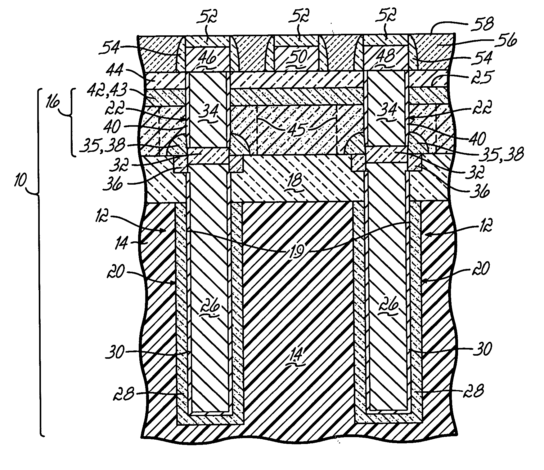
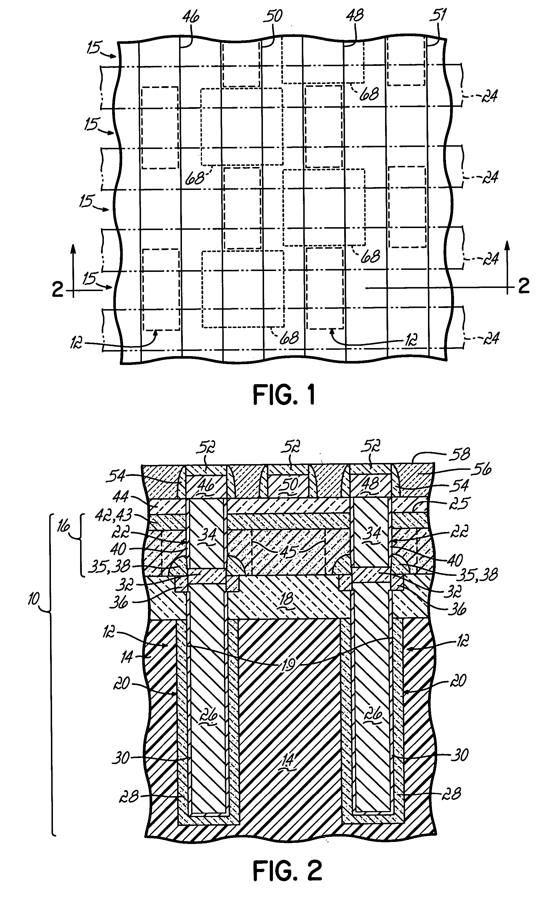
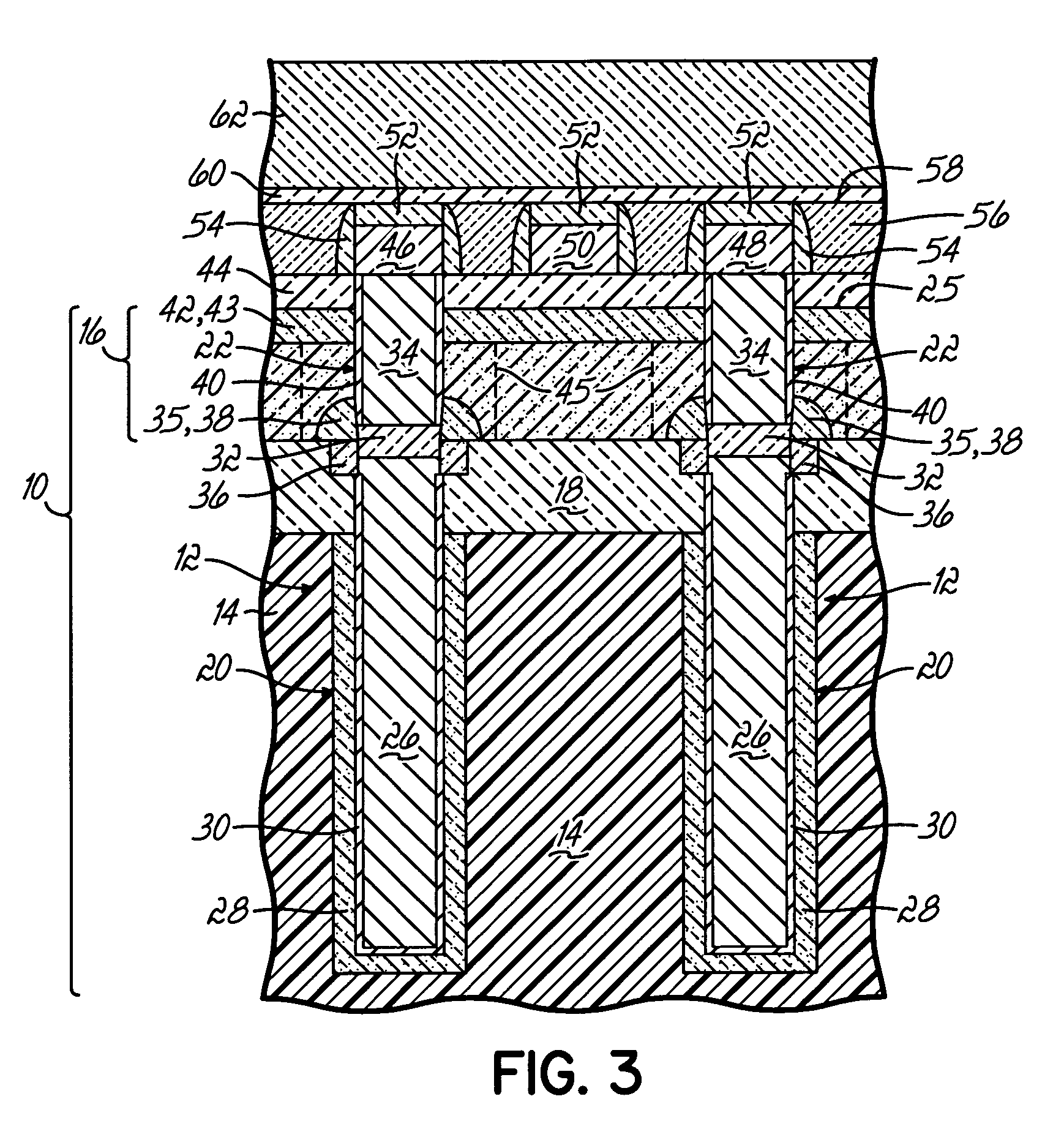
[0021] The present invention provides a semiconductor structure including an array of vertical memory cells built using semiconductor-on-insulator (SOI) technology, as well as methods of making such semiconductor structures. Specifically, the access device for at least one vertical memory cell and, typically, every vertical memory cell in the memory cell array has an associated relatively high-resistance body contact established through the buried insulating or dielectric layer separating the floating SOI body of an SOI wafer, in which the access device is built, from the underlying semiconductor substrate. The present invention may be particularly applicable and beneficial for merged isolation and node trench (MINT) memory cells, although the invention is not so limited. The requisite high resistance for the body contact may be achieved by creating a localized silicon rich oxide (SRO) region of relatively high resistance in the buried dielectric layer. The present invention will no...


PUM


Abstract

A semiconductor structure for a dynamic random access memory (DRAM) cell array that includes a plurality of vertical memory cells built on a semiconductor-on-insulator (SOI) wafer and a body contact in the buried dielectric layer of the SOI wafer. The body contact electrically couples a semiconductor body with a channel region of the access device of one vertical memory cell and a semiconductor substrate of the SOI wafer. The body contact provides a current leakage path that reduces the impact of floating body effects upon the vertical memory cell. The body contact may be formed by an ion implantation process that modifies the stoichiometry of a region of the buried dielectric layer so that the modified region becomes electrically conductive with a relatively high resistance.

Description

CROSS-REFERENCE TO RELATED APPLICATIONS [0001] This application is related to commonly-assigned Application Ser. No. ______ , filed on even date herewith, entitled “SEMICONDUCTOR STRUCTURES WITH BODY CONTACTS AND FABRICATION METHODS THEREOF” and bearing Attorney Docket No. ROC920050178US1, which is hereby incorporated by reference herein in its entirety.FIELD OF THE INVENTION [0002] The invention relates generally to semiconductor structures and, in particular, to semiconductor structures with multiple vertical memory cells arranged to form a memory array and methods of forming such semiconductor structures. BACKGROUND OF THE INVENTION [0003] Dynamic random access memory (DRAM) devices are the most commonly used type of semiconductor memory and, thus, are found in many integrated circuit designs. DRAM devices are also frequently embedded into application specific integrated circuits, such as processors and logic devices. A generic DRAM device includes a plurality of substantially id...

Claims


Application Information

Patent Timeline
IPC IPC(8): H01L27/108
CPCH01L21/84H01L27/0218H01L29/66545H01L27/1203H01L27/10841H10B12/395
Inventor CHENG, KANGGUOHSU, LOUIS LU-CHENMANDELMAN, JACK ALLAN
Owner IBM CORP
Why Eureka
Try Eureka